Preparation method for small silicon-based nano hollow array with orderly heights

A highly ordered, small-scale technology, used in the manufacture of microstructure devices, processes for producing decorative surface effects, decorative arts, etc. Easy operation control, highly ordered arrangement, low equipment price and low production cost

Inactive Publication Date: 2011-09-07
FUDAN UNIV
View PDF5 Cites 48 Cited by
  • Summary
  • Abstract
  • Description
  • Claims
  • Application Information

AI Technical Summary

Problems solved by technology

However, the size of the nanopit described in the report is large and...

Method used


Image

  • Preparation method for small silicon-based nano hollow array with orderly heights
  • Preparation method for small silicon-based nano hollow array with orderly heights
  • Preparation method for small silicon-based nano hollow array with orderly heights

Examples


Embodiment Construction

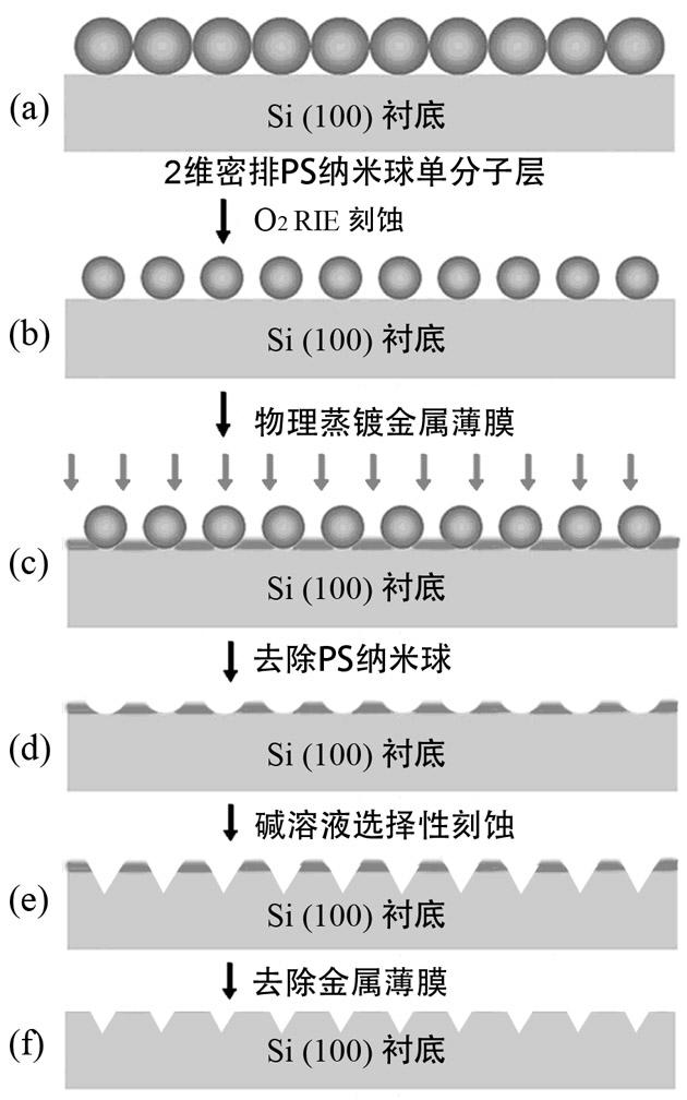
[0027] 1. The substrate is Si(001) single wafer. Carry out the following cleaning treatment: rinse with deionized water for 2 minutes, sonicate with acetone for 5 minutes, and sonicate with methanol for 5 minutes. Rinse with deionized water for 5 minutes. in H 2 SO 4 :H 2 o 2 =2:1 After boiling the solution for 5 minutes, continue to soak for 5 minutes. After rinsing with deionized water for 3 minutes, put the ratio of HF:H 2 Dip in O=1:9 solution for 60 seconds to remove the oxide layer on the surface of the silicon wafer. Finally, after rinsing with deionized water for 60 seconds, spin dry with a spinner.

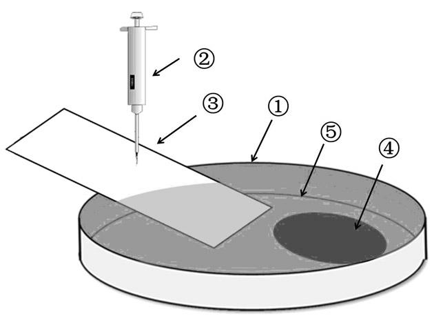
[0028] 2. To cover a single layer of polystyrene nanospheres on a silicon substrate, establish as figure 2 installation. The petri dish is made of polystyrene. The size is 100mm×20mm.

[0029] 3. will figure 2The slides used in the shown device were cleaned as follows: rinse with deionized water for 2 minutes, sonicate with acetone for 5 minutes, sonicate with...


PUM

PropertyMeasurementUnit
Diameteraaaaaaaaaa
Densityaaaaaaaaaa

Abstract

The invention relates to a preparation method for a small silicon-based nano hollow array with orderly heights, belonging to the technical field of nano-structure preparation. The preparation method employs large-diameter polystyrene nano-spheres which are self-mounted into a single-layer nano-sphere film serving as masks on a Si substrate. After going through multiple technical procedures such as reaction ion lithography, direct current sputtering metal films, selective corrosion and the like, the mask is converted into a small inverted-pyramidal nano-hollow array, which is a two-dimensionalhexagonal dot array. The cycle of the nano-hollow arrays is determined by the diameters initially selected for the polystyrene nano-spheres. The invention is likely to be used in fields of growth of controllable quantum structures, photonic crystal manufacturing, quantum logic operation, magnetic storage media, etc.

Description

technical field [0001] The invention belongs to the technical field of nanostructure preparation, and in particular relates to a method for preparing a small-size silicon-based nanopit array. Background technique [0002] In recent years, with the continuous development and maturity of various semiconductor integration processes, the preparation and characterization of semiconductor low-dimensional nanomaterials have also made great progress, and have gradually entered into practical use. Semiconductor low-dimensional quantum structures (such as quantum dots, quantum wires, quantum rings, etc.) present many novel physical properties due to the quantum confinement effect caused by low spatial dimensions and extremely small sizes, and become the current research field in the field of low-dimensional nanostructures. One of the hot spots. However, the quantum structure grown by self-assembly technology is generally difficult to precisely control its spatial distribution, shape ...

Claims


Application Information

Patent Timeline
IPC IPC(8): B81C1/00
Inventor 钟振扬马英杰崔健樊永良蒋最敏
Owner FUDAN UNIV
Why Eureka
Try Eureka