
Method for growing ordered silicon-based germanium quantum dots

A quantum dot, silicon-based technology, applied in the field of growing ordered silicon-based germanium quantum dots, to achieve the effect of improving size uniformity

Active Publication Date: 2011-09-28
ZHEJIANG UNIV
View PDF3 Cites 12 Cited by
  • Summary
  • Abstract
  • Description
  • Claims
  • Application Information

AI Technical Summary

Problems solved by technology

But in general, it is still a big challenge to obtain a satisfactory structure by using traditional lithography technology to obtain a quantum dot structure with a size smaller than 50nm and arrange it in an ordered array.

Method used


Image

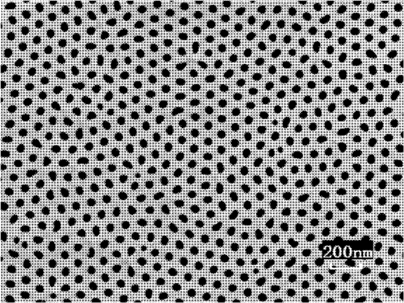
  • Method for growing ordered silicon-based germanium quantum dots
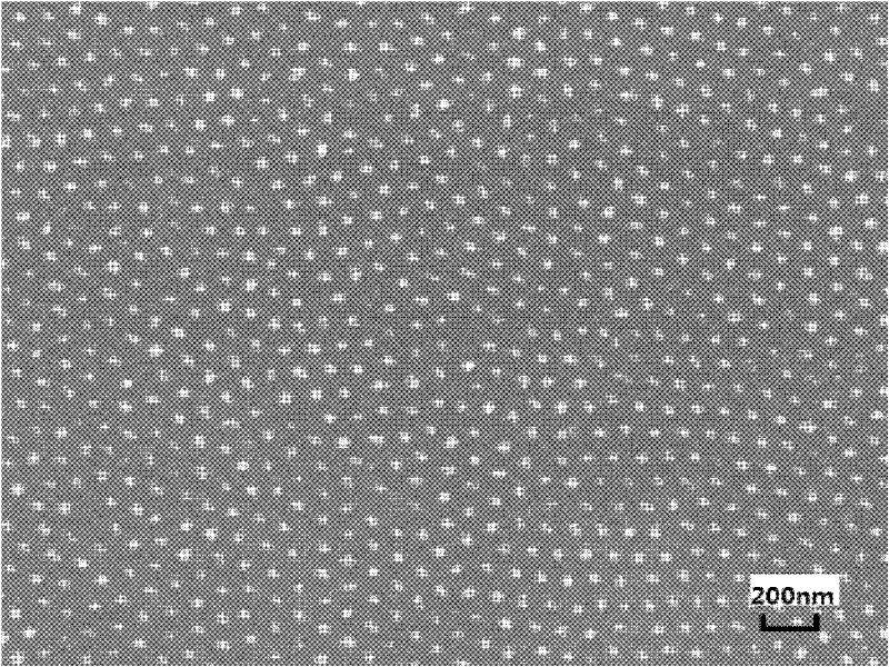
  • Method for growing ordered silicon-based germanium quantum dots
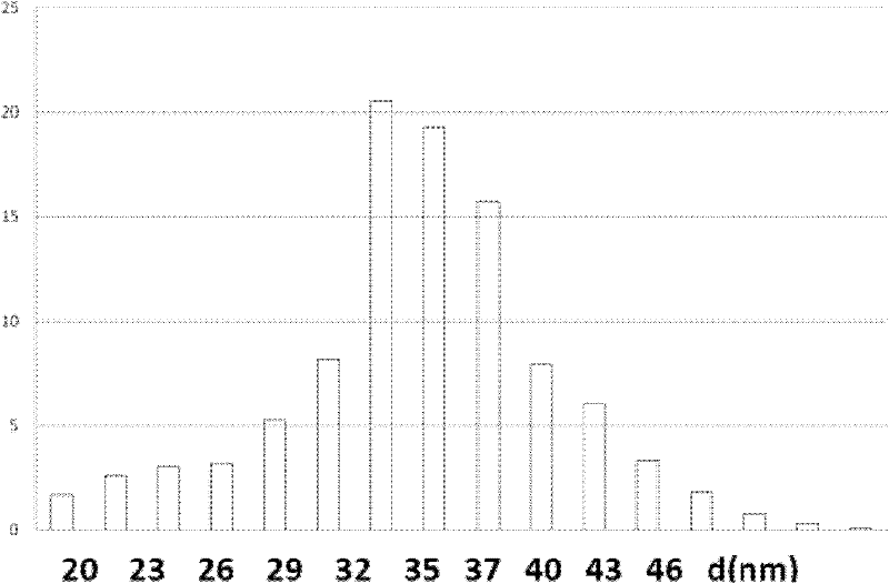
  • Method for growing ordered silicon-based germanium quantum dots

Examples


Embodiment 18

[0029] (1) Two-inch single-polished p-type (111) silicon wafers are cleaned by RCA to obtain a clean surface, and are covered with a thin oxide layer; the oxide layer is dense SiO 2 ;

[0030] Wherein, the RCA cleaning step is: ultrasonic cleaning with acetone solution for 10 minutes, and then rinsing with deionized water; aqueous ammonia hydrogen peroxide solution (by volume ratio, NH 4 OH:H 2 o 2 :H 2 (0=1:1:5) boiled for 10 minutes, rinsed repeatedly with deionized water; soaked in HF (4% by mass) solution for 1 minute, rinsed with deionized water; hydrochloric acid hydrogen peroxide solution (in volume ratio, HCl:H 2 o 2 :H 2 (0=1:1:5) boiled for 10 minutes, rinsed repeatedly with deionized water; repeated two to three rounds of soaking in HF solution and boiling in hydrochloric acid hydrogen peroxide solution for two to three rounds, then sealed with deionized water and dried with nitrogen before use.

[0031] (2) stick the porous aluminum oxide film on the surface ...

Embodiment 28

[0039] (1) Two-inch single-polished p-type (111) silicon wafers are cleaned by RCA to obtain a clean surface, and are covered with a thin oxide layer; the oxide layer is dense SiO 2 ;

[0040] Wherein, the RCA cleaning step is: ultrasonic cleaning with acetone solution for 10 minutes, and then rinsing with deionized water; aqueous ammonia hydrogen peroxide solution (by volume ratio, NH 4 OH:H 2 o 2 :H 2 (0=1:1:5) boiled for 10 minutes, rinsed repeatedly with deionized water; soaked in HF (4% by mass) solution for 1 minute, rinsed with deionized water; hydrochloric acid hydrogen peroxide solution (in volume ratio, HCl:H 2 o 2 :H 2 (0=1:1:5) boiled for 10 minutes, rinsed repeatedly with deionized water; repeated two to three rounds of soaking in HF solution and boiling in hydrochloric acid hydrogen peroxide solution for two to three rounds, then sealed with deionized water and dried with nitrogen before use.

[0041] (2) The porous aluminum oxide film is pasted on the surf...


PUM

PropertyMeasurementUnit
thicknessaaaaaaaaaa
diameteraaaaaaaaaa
sizeaaaaaaaaaa

Abstract

The invention discloses a method for preparing high-density and ordered germanium quantum dots on a silicon substrate, which comprises the following steps of: adhering porous anodic aluminum oxide on a surface of a silicon wafer cleaned by an RCA (Remote Control Adapter); putting the silicon wafer in molecular beam epitaxial growth equipment for growing the germanium quantum dots after through holes are arranged on the silicon wafer; and removing a template through a high-temperature annealing process to leave periodically arranged germanium quantum dot structures. When the method disclosed by the invention is adopted, the high-density and ordered germanium quantum dots can be obtained.

Description

technical field [0001] The invention belongs to the field of nano material structure preparation and relates to a method for growing ordered silicon-based germanium quantum dots. Background technique [0002] With the development of integrated circuits, silicon-based microelectronic chips have formed a huge scale industry, and have become the dominant force in today's information industry and a major pillar of the information society. With the reduction of the scale of the device to the nanometer level and the reduction of the number of electrons contained in the device, the conventional working mode of the device will be affected, and the quantum effect will become more and more obvious. Therefore, quantum devices with nanometer dimensions will likely become the basic components of VLSI in the future, and growing germanium quantum dots on silicon substrates is an important way to solve the above problems. [0003] Germanium quantum dots have been widely studied in silicon-...

Claims


Application Information

Patent Timeline
Patent Type & Authority Applications(China)
IPC IPC(8): B82Y40/00H01L31/18
CPCY02P70/50
Inventor 叶辉张磊皇甫幼睿詹文博
Owner ZHEJIANG UNIV
Learn More