Manufacturing method for ohmic contact with low specific contact resistance and low roughness
A technology of ohmic contact and manufacturing method, applied in the field of low-roughness ohmic contact manufacturing and low-specific contact resistance, can solve the problems of poor Mo thickness and evaporation conditions, and metal warping and peeling off, so as to improve the overlay accuracy and improve the Stable, easy to achieve results
- Summary
- Abstract
- Description
- Claims
- Application Information
AI Technical Summary
Problems solved by technology
Method used
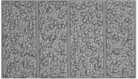
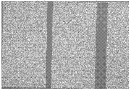
Image

Examples
Embodiment Construction
[0021] The present invention will be further described in detail below in conjunction with the accompanying drawings and specific embodiments.
[0022] A manufacturing method of low specific contact resistance and low roughness ohmic contact, characterized in that said manufacturing method comprises the following steps:
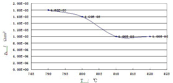
[0023] A. Evaporation to form ohmic contact: Put the clean metal source (including metal Ti, Al, Ni, Mo and Au) into the crucible of the electron beam evaporation table, and then perform the melting source process to make the metal meet the evaporation needs. Afterwards, place the GaN epitaxial material wafer with photolithographic ohmic contact pattern on the planet carrier of the electron beam evaporation table, and wait for the vacuum degree in the chamber of the electron beam evaporation table to reach 7×10 -7 Torr, according to the order of Ti, Al, Ni, Mo, Au, the metal evaporation process is performed sequentially to form an ohmic contact;
[0024] B. ...
PUM
 Abstract
Description
Claims
Application Information
 - R&D
- Intellectual Property
- Life Sciences
- Materials
- Tech Scout
- Unparalleled Data Quality
- Higher Quality Content
- 60% Fewer Hallucinations
Browse by: Latest US Patents, China's latest patents, Technical Efficacy Thesaurus, Application Domain, Technology Topic, Popular Technical Reports.
© 2025 PatSnap. All rights reserved.Legal|Privacy policy|Modern Slavery Act Transparency Statement|Sitemap|About US| Contact US: help@patsnap.com