Solar cell and manufacturing method thereof

A technology of solar cells and manufacturing methods, applied in the direction of final product manufacturing, sustainable manufacturing/processing, circuits, etc., can solve the problems of low efficiency of solar cells, reduced passivation effect, hydrogen atom escape, etc., to achieve firm combination, passivation Good chemical effect and high treatment temperature

Inactive Publication Date: 2011-11-16
BEIJING NAURA MICROELECTRONICS EQUIP CO LTD
View PDF9 Cites 11 Cited by
  • Summary
  • Abstract
  • Description
  • Claims
  • Application Information

AI Technical Summary

Problems solved by technology

[0005] However, the inventors have found that at least the following problems exist in the prior art: in the existing solar cell manufacturing method, high-temperature sintering at a temperature of 800-900°C is required after forming the silicon nitride anti-reflection film, so a large amount of hydrogen atoms will It escapes during high temperature sintering, reducing the passivation effect, resulting in low efficiency of the solar cells produced

Method used


Image

  • Solar cell and manufacturing method thereof
  • Solar cell and manufacturing method thereof
  • Solar cell and manufacturing method thereof

Examples


Embodiment 1

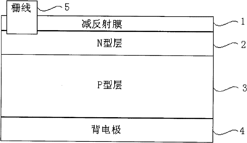
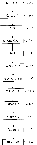
[0023] like image 3 As shown, the embodiment of the present invention provides a solar cell manufacturing method (taking the manufacturing method of a crystalline silicon solar cell as an example), which includes the following steps:

[0024] S01, silicon wafer (solar cell substrate) cleaning: clean the bare silicon wafer;

[0025] S02. Surface corrosion: use 10-30% alkali solution to corrode silicon wafers at 80-100°C for 0.5-1min to remove oil stains, cutting damage layers, etc., and the corrosion rate can reach 6-10μm / min.

[0026] S03. Texturing: Form a textured surface (similar to an inverted pyramid-shaped surface texture) on the surface of the silicon wafer by mechanical grooving, chemical etching, reactive ion etching, laser grooving, etc., to reduce surface reflection loss.

[0027] S04, PN junction by diffusion method: Transport the carrier gas carrying the required doped impurities to the surface of the silicon wafer, diffuse the impurities to a depth of about sev...

Embodiment 2

[0037] like image 3 As shown, the embodiment of the present invention provides a solar cell manufacturing method (taking the manufacturing method of a crystalline silicon solar cell as an example), which includes the following steps:

[0038] S01, silicon wafer (solar cell substrate) cleaning: clean the bare silicon wafer;

[0039] S02. Surface corrosion: use 10-30% alkali solution to etch the silicon wafer at 80-100° C. for 0.5-1 min.

[0040] S03. Texturing: forming a textured surface (similar to an inverted pyramid-shaped surface texture) on the surface of the silicon wafer by mechanical grooving, chemical etching, reactive ion etching, laser grooving and other methods.

[0041] S04, PN junction by diffusion method: Transport the carrier gas carrying the required doped impurities to the surface of the silicon wafer, diffuse the impurities to a depth of about several hundred nanometers, and then perform high temperature treatment to continue to diffuse the impurity atoms i...

Embodiment 3

[0051] The solar cell manufacturing method of this embodiment is similar to the above embodiment, the difference is:

[0052] In the hydrogen treatment step (S06), the chamber is evacuated to 0.5 Pa, and hydrogen gas (that is, hydrogen-containing gas) with a flow rate of 8000 sccm is introduced, and the pressure is controlled at 500 Pa, heated to 1500 ° C and treated for 10 s;


PUM


Abstract

The invention provides a solar cell and a manufacturing method thereof, belongs to the technical field of solar cells, and can solve the problem that the conventional solar cell is low in efficiency. The solar cell manufacturing method comprises the step of performing hydrogen treatment on a solar cell substrate, wherein the hydrogen treatment comprises the step of treating the solar cell substrate at the temperature of 800 to 1,500 DEG in hydrogen atmosphere. The solar cell is subjected to hydrogen treatment during manufacturing. The solar cell can be used for a crystalline silicon solar cell.

Description

technical field [0001] The invention relates to a solar cell and a manufacturing method thereof, in particular to a crystalline silicon solar cell and a manufacturing method thereof. Background technique [0002] As a clean energy source, solar cells are used more and more widely. Conventional solar cells have such figure 1 In the structure shown, the substrate of the solar cell includes a PN junction, and the two sides of the PN junction respectively have an anti-reflection film 1 (usually a silicon nitride film) and a back electrode 4, and there is a front electrode 5 (grid line) on the anti-reflection film 1. ), the front electrode 5 will pass through the anti-reflection film 1 and be in contact with the substrate of the solar cell during the high-temperature sintering step of cell preparation. [0003] The efficiency (photoelectric conversion efficiency) of a solar cell is its most important performance, and the loss of solar cell efficiency mainly includes light loss a...

Claims


Application Information

Patent Timeline
Patent Type & Authority Applications(China)
IPC IPC(8): H01L31/18H01L31/052H01L31/068
CPCY02E10/50Y02E10/547Y02P70/50
Inventor 荣延栋
Owner BEIJING NAURA MICROELECTRONICS EQUIP CO LTD
Why Eureka
Try Eureka