Light-focusing device and manufacturing method thereof as well as solar cell system
A technology of a solar cell and a concentrating device, which is applied in the field of light energy, can solve the problems of aging, difficulty in absorbing and utilizing light, and low photoelectric conversion efficiency of solar cells.
- Summary
- Abstract
- Description
- Claims
- Application Information
AI Technical Summary
Problems solved by technology
Method used
Image
Examples
Embodiment 1
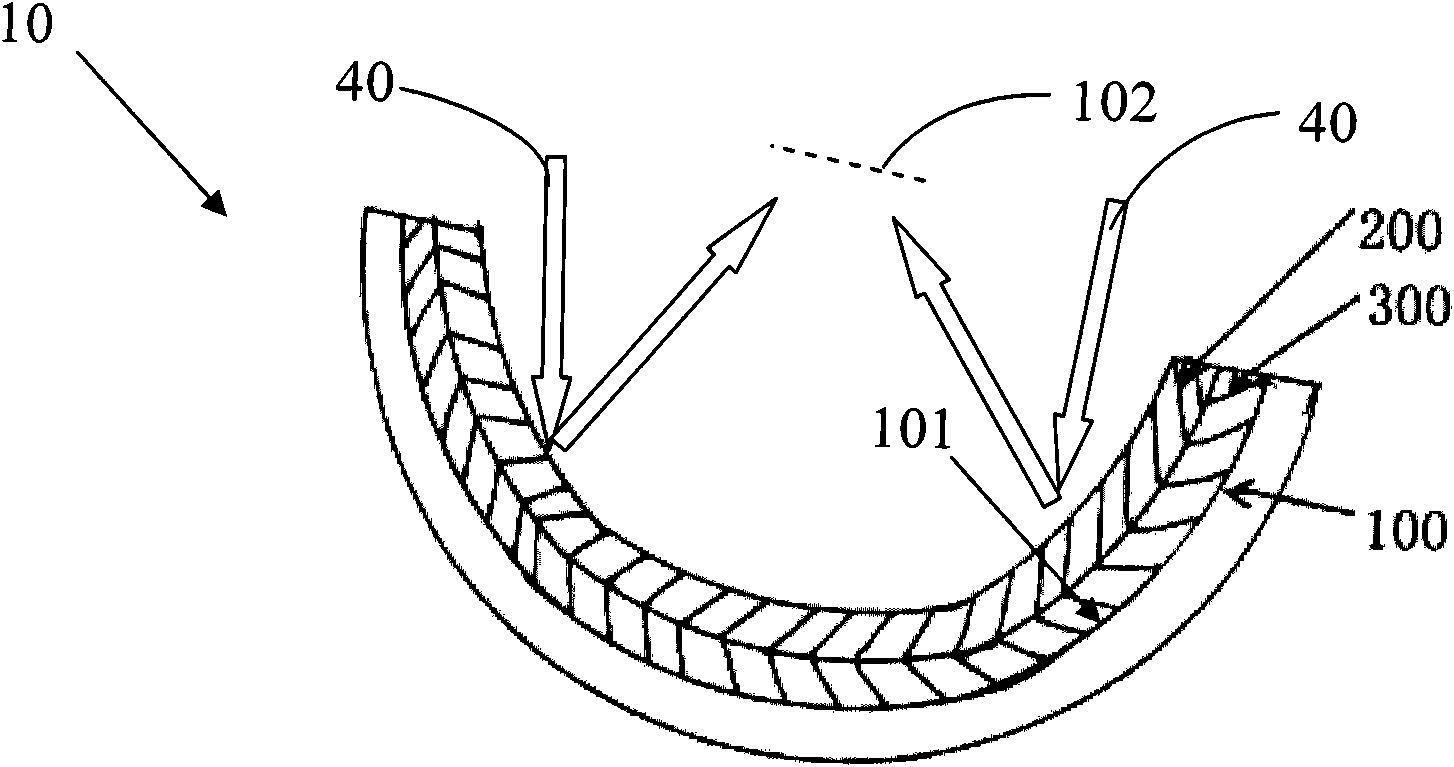
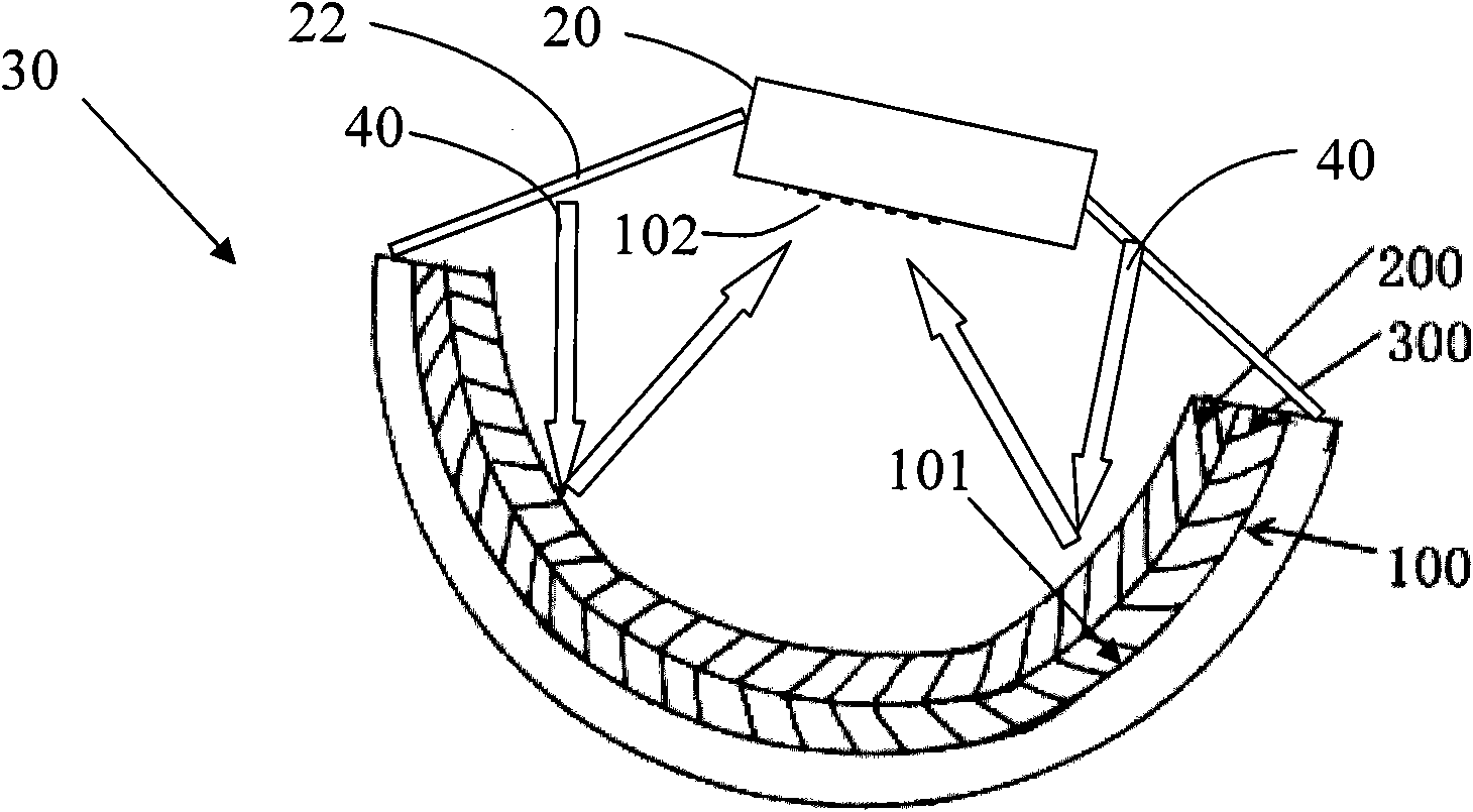
[0045] The structure of the light concentrating device of this embodiment is as follows: figure 1 As shown, wherein the concentrating substrate 100 adopts concave glass with a parabolic concave surface of revolution 101, and the photonic crystal layer 300 adopts monodisperse polymer latex particles with a hard core-soft shell structure, and the particle size of the particles is about 650nm. The thickness of the crystal layer 300 is about 1000 nanometers. The down conversion material of the down conversion layer 200 is poly-N-vinylacetamide europium(III) which is a rare earth co-luminescent organic complex. The thickness of the down conversion layer 200 is about 0.1 μm.
[0046] The specific manufacturing process of the light concentrating device of the above-mentioned embodiment is as follows:
[0047] (1) Prepare a piece of concave glass as a substrate, wash it and dry it for later use;
[0048](2) according to the preparation method that the Chinese patent that application ...
Embodiment 2
[0051] The structure of the light concentrating device of this embodiment is as follows: figure 1 As shown, wherein the concentrating substrate 100 adopts concave organic glass with a parabolic concave surface of revolution 101, and the photonic crystal layer 300 adopts monodisperse polymer latex particles with a hard core-soft shell structure, and the particle size of the particles is about 500nm. The thickness of the photonic crystal layer 300 is about 1000 nanometers, and the down conversion material of the down conversion layer 200 is Eu 3+ Doped LiGdF 4 As a thin film, the thickness of the down conversion layer 200 is about 20 μm.
[0052] The specific manufacturing process of the light concentrating device of the above-mentioned embodiment is as follows:
[0053] (1) Prepare a piece of concave plexiglass as a substrate, clean it and dry it for later use;
[0054] (2) According to the preparation method provided by the Chinese patent with the application number 2005100...
Embodiment 3
[0057] The structure of the light concentrating device of this embodiment is as follows: figure 1 As shown, wherein the concentrating substrate 100 is made of concave plastic with a parabolic concave surface of revolution 101, and the photonic crystal layer 300 is made of SiO 2 and TiO 2 , the thickness of the photonic crystal layer 300 is about 480 nanometers, and the down conversion material of the down conversion layer 200 adopts Y 3 al 5 o 12 : Ce 3+ , the thickness of the down conversion layer 200 is about 10 μm.
[0058] The specific manufacturing process of the light concentrating device of the above-mentioned embodiment is as follows:
[0059] (1) Prepare a piece of concave plastic as the substrate, wash it and dry it for later use;
[0060] (2) According to the preparation method provided by the Chinese patent application number 200410018081, SiO is alternately grown on the substrate by ultra-high vacuum electron beam evaporation 2 and TiO 2 Thin film, 8 layer...
PUM
| Property | Measurement | Unit |
|---|---|---|
| thickness | aaaaa | aaaaa |
| thickness | aaaaa | aaaaa |
| particle size | aaaaa | aaaaa |
Abstract
Description
Claims
Application Information


