Organic thin film transistor using paper substrate and silk dielectric layer and manufacturing method thereof

A technology of organic thin film and production method, which is applied in the fields of electrical solid-state devices, semiconductor/solid-state device manufacturing, circuits, etc., can solve the problems of pentacycline carrier mobility, poor matching, and expensive equipment, etc., and achieve effective Conducive to large-area production, improved transistor characteristics, simple and cheap process

Inactive Publication Date: 2011-12-07
NATIONAL TSING HUA UNIVERSITY
View PDF6 Cites 4 Cited by
  • Summary
  • Abstract
  • Description
  • Claims
  • Application Information

AI Technical Summary

Problems solved by technology

[0005] The known gate dielectric layer mainly uses sputtering to form dielectric materials on the substrate and gate, so it often faces problems such as expensive equipment and complicated processes.
In addition, the best organic semiconductor layer material commonly used in organic thin film transistors is pentacycline, but because of the poor match between commonly used dielectric materials and pentacycline, the carrier mobility of pentacycline is low
For example, the pentacycline organic thin film transistor generally uses silicon oxide as the material of the gate dielectric layer, and its pentacycline carrier mobility is less than 0.5 cm 2 / V-sec; and even when the currently known good aluminum nitride dielectric material is used as the gate dielectric layer material, the pentacycline carrier mobility of the pentacycline organic thin film transistor cannot be higher than 2cm 2 / V-sec
Therefore, with existing technologies and materials, it is still impossible to produce organic thin film transistors with high efficiency.
[0006] At the same time, although ordinary flexible plastic substrates can be used to produce flexible and rollable organic thin film transistor devices, due to the awareness of environmental protection has been highly valued by the world, if plastic materials are used, it may be difficult to recycle and cause damage. Disadvantages of environmental pollution
Organic thin film transistors based on paper are an option, but due to the limitation of process temperature and the limited selection of dielectric layer materials for paper substrates, the carrier mobility of organic thin film transistors based on paper is currently low. For example , People such as Florian Eder of Germany in 2004, disclosed in Applied Physics Letters periodical (Applied Physics Letters 84,2673-2675 (2004)) take paper as substrate and take polyvinylphenol (polyvinylphenol, PVP) as dielectric layer material five The characteristics of cyclocycline organic thin film transistors, the pentacycline carrier mobility is only about 0.2cm 2 / V-sec

Method used


Image

  • Organic thin film transistor using paper substrate and silk dielectric layer and manufacturing method thereof
  • Organic thin film transistor using paper substrate and silk dielectric layer and manufacturing method thereof
  • Organic thin film transistor using paper substrate and silk dielectric layer and manufacturing method thereof

Examples


Embodiment 1

[0026] Example 1 - Top Contact Organic Thin Film Transistor Device

[0027] Preparation of silk aqueous solution

[0028] Firstly, prepare an aqueous solution containing 10wt% sodium carbonate, heat to boil, add dry natural silk, and boil for 30 minutes to remove sericin on the outer layer of silk. Then, put it into deionized water for washing to wash away the lye attached to the outer layer of silk. After drying, refined silk can be obtained, that is, fibroin.

[0029] Next, put the scoured silk into 20ml of 85wt% phosphoric acid solution, and stir until dissolved. Then, the phosphoric acid solution in which the silk was dissolved was placed in a dialysis membrane (Spectra / Por 3 dialysis membrane, molecular weight cutoff = 14000) and dialyzed for 3 days to remove the phosphoric acid solution. Finally, filter out impurities with filter paper to obtain an aqueous silk solution.

[0030] Fabrication of Top-Contact Organic Thin Film Transistor Devices

[0031] First, if Fi...

Embodiment 2 1

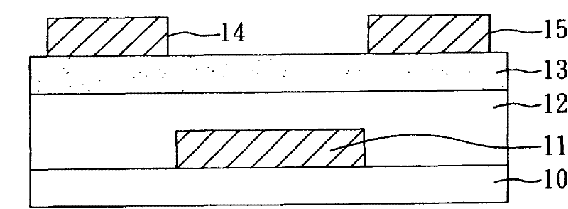
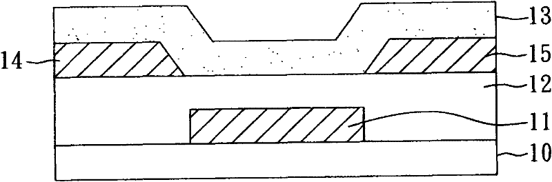
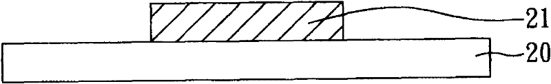
[0046] Embodiment 2 One contact type organic thin film transistor device

[0047] like Figure 5A As shown, a paper substrate 20 is provided, and a gate electrode 21 and a gate dielectric layer 22 are sequentially formed on the paper substrate 20 . In this embodiment, the materials and preparation methods of the paper substrate 20 , the grid 21 , and the gate dielectric layer 22 are the same as those in the first embodiment. In addition, in this embodiment, the thickness of the gate 21 is about 100 nm, and the thickness of the gate dielectric layer 22 is about 500 nm.

[0048] Next, if Figure 5B As shown, a patterned metal layer is vapor-deposited on the gate dielectric layer 22 to serve as the source 24 and the drain 25 by using the same process conditions as in the embodiment 1 for forming the gate. In this embodiment, the material of the source electrode 24 and the drain electrode 25 is gold, and its thickness is about 100 nm.

[0049] Finally, if Figure 5C As shown,...


PUM


Abstract

The invention relates to an organic thin film transistor using a paper substrate and a silk dielectric layer and a manufacturing method thereof. Wherein, the organic thin film transistor device includes: a paper substrate; a gate, which is arranged on the paper substrate; a gate dielectric layer, which is arranged on the paper substrate and covers the gate, wherein the material of the gate dielectric layer is It includes a fibroin; an organic semiconductor layer; and a source and a drain, wherein the organic semiconductor layer, the source and the drain are arranged on the gate dielectric layer.

Description

technical field [0001] The present invention relates to an organic thin film transistor device and its manufacturing method, especially to an organic thin film transistor using paper substrate and silk dielectric layer and its manufacturing method, so that the organic thin film transistor device can be flexible and rollable sex. Background technique [0002] In recent years, thin film transistors (TFTs) have been widely used in sensors, electronic tags (RFID) and display devices. In order to reduce the production cost of the product and expand the application range of the product, an organic thin film transistor (OTFT) that is low-cost, flexible, and can be produced in a large area is a research and development trend. [0003] In general, organic thin film transistors can be classified into top-contact organic thin film transistors and bottom-contact organic thin film transistors. like Figure 1A As shown, the top-contact organic thin film transistor includes: a substrate ...

Claims


Application Information

Patent Timeline
Patent Type & Authority Applications(China)
IPC IPC(8): H01L51/05H01L51/30H01L51/40
Inventor 黄振昌王中桦谢兆莹
Owner NATIONAL TSING HUA UNIVERSITY
Why Eureka
Try Eureka