Device for directionally emitting enhanced Raman spectrums by utilizing surface plasmas

A technology of surface plasmon and directional emission, which is applied in measurement devices, Raman scattering, material excitation analysis, etc., can solve the problems of unfavorable integration, miniaturization, and complex instrument structure, and meet the requirements of reducing collection distance and numerical aperture , simple operation steps, and the effect of improving collection efficiency

Inactive Publication Date: 2011-12-14
JILIN UNIV
View PDF10 Cites 37 Cited by
  • Summary
  • Abstract
  • Description
  • Claims
  • Application Information

AI Technical Summary

Problems solved by technology

However, the excitation light and the detected Raman signal are located on different sides of the metal film, and the instrument structure is relatively complicated, which is not conducive to the realization of integration and miniaturization

Method used


Image

  • Device for directionally emitting enhanced Raman spectrums by utilizing surface plasmas
  • Device for directionally emitting enhanced Raman spectrums by utilizing surface plasmas
  • Device for directionally emitting enhanced Raman spectrums by utilizing surface plasmas

Examples


Embodiment 1

[0028] Embodiment 1: Determining the SPR angle under different conditions

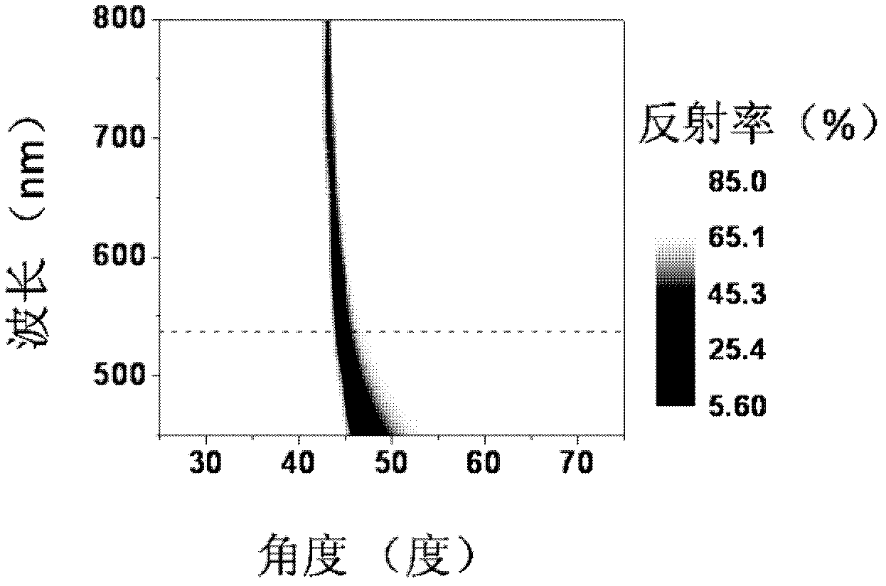
[0029] Such as figure 2 As shown, the excitation light source 1 emits P-polarized white parallel light with a wavelength range of 350-800 nanometers; the dielectric layer 2 is a semi-cylindrical BK7 glass prism, and the multilayer film system 3 is a silver film with a thickness of 350 nm. The medium layer 4 is air;

[0030]The P-polarized white light parallel light source 1 is incident at the junction of the prism 2 and the silver film 3 at different incident angles, and reflection and refraction occur. The convex lens 6 and the spectrometer 7 detect the reflected light at different acceptance angles, and the acceptance angle is always set equal to the incident angle. Change it every 1 degree from 25 degrees to 80 degrees, so that you can get the reflectivity at different angles.

[0031] Figure 3 is figure 2 The reflectance spectrum measured by the device. Figure 3a for figure 2 In the reflec...

Embodiment 2

[0034] Figure 4a It is a structural schematic diagram of a device for SERS detection based on a semi-cylindrical prism;

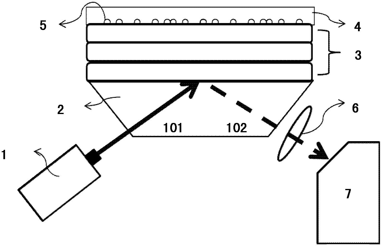
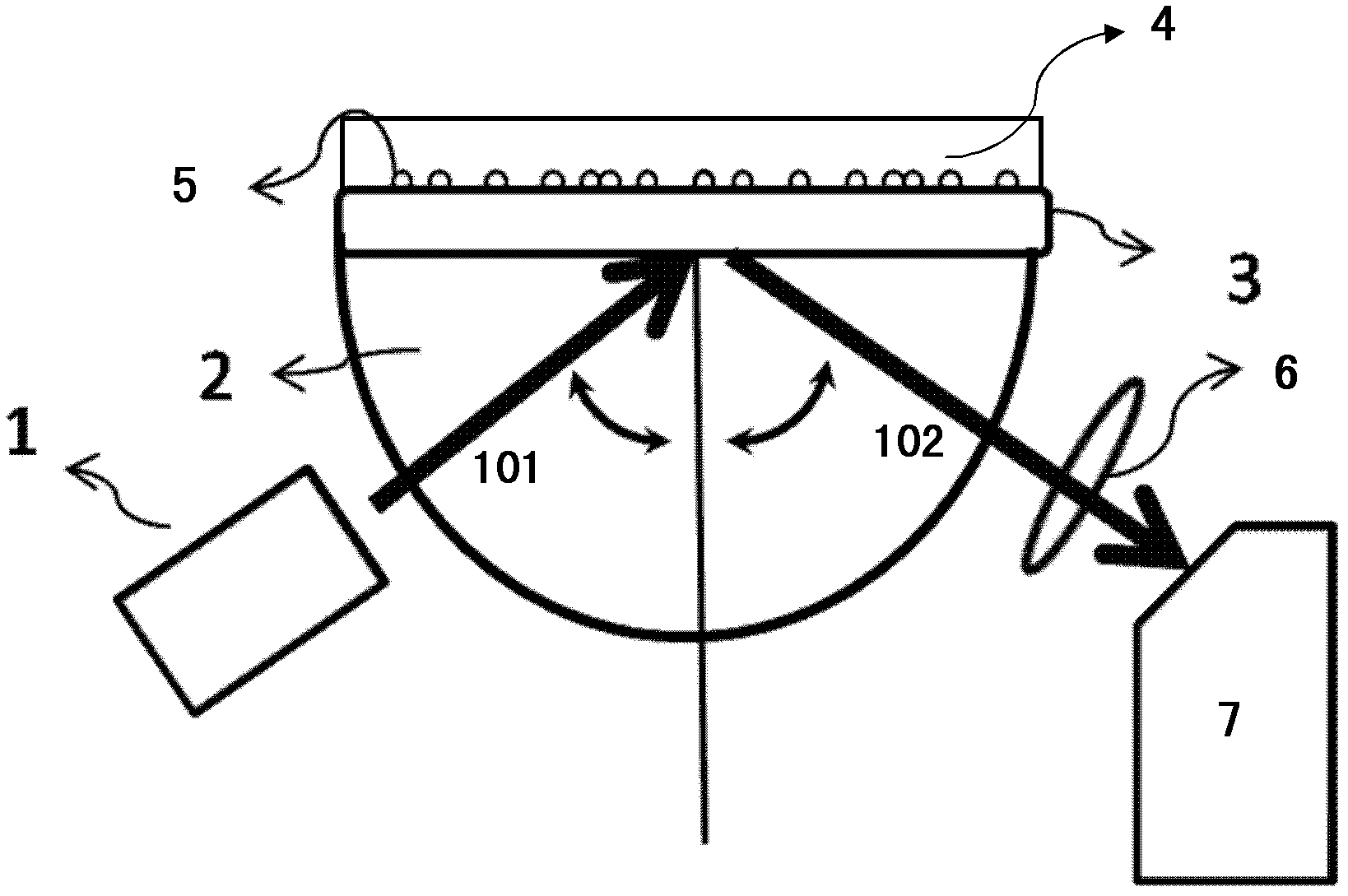
[0035] The excitation light source 1 is a semiconductor laser with a wavelength of 532nm, the power is 15mW, the dielectric layer 2 is a semi-cylindrical prism made of BK7 material, and the multilayer film system 3 is a single-layer silver film with a thickness of 50nm, which is prepared on the prism by vacuum evaporation. get. The receiving device is composed of a long-pass filter 8 , a convex lens 6 and a spectrometer 7 . Sample 5 to be tested is p-mercaptoaniline molecule, the concentration is 10 -4 mol / L, assembled on the silver film by seed soaking method. Spectrometer 7 is an image-enhanced CCD spectrometer from Princeton Instruments, which can amplify the optical signal by about 700 times. The numerical aperture of the excitation lens and the detection lens in the excitation and detection device is about 0.03.

[0036] Figure 4b The incident ...

Embodiment 3

[0041] Figure 5a It is a schematic structural diagram of a device for SERS detection based on the reflective layer 12 on the surface of the dielectric layer 2 .

[0042] Here is a detailed introduction to the incident and inspection device (the dotted box in the figure), and several other implementation methods Figure 5b -e can be designed with a device similar to that here.

[0043] The excitation light source 1 is a 532nm solid-state laser, the dielectric layer 2 is a semi-cylindrical prism 2 made of BK7 material, the reflection layer 12 and the incident excitation light are distributed on both sides of the normal line of the bottom surface of the prism, and the reflection layer is 300nm by vacuum evaporation or sputtering. Thick silver or aluminum film, the incident luminescence emitted by the exciting light source (1) passes through the dichroic filter 10 of Semrock Company, and then converges on the interface between the multilayer film system 3 and the prism through t...


PUM

PropertyMeasurementUnit
thicknessaaaaaaaaaa
thicknessaaaaaaaaaa
thicknessaaaaaaaaaa

Abstract

The invention belongs to the technical field of surface enhanced Raman spectrums, in particular to a device for directionally emitting enhanced Raman spectrums by utilizing surface plasmas. A dielectric layer is arranged at one side of a multilayered film system; a to-be-measured sample is arranged at the other side of the multilayered film system; the multilayered film system comprises at least one layer of metal film; an exciting light sent by an excitation light source enters into the multilayered film system from the dielectric layer along a SPR (Surface Plasmon Resonance) angle; Raman signals in the to-be-measured sample are absorbed by the metal film and then the surface plasmas in the metal film are excited again; the surface plasmas carrying the Raman signals are coupled and emitted at the boundary between the dielectric layer and the multilayered film system; the emitting directions of the surface plasmas are also along the SPR angle; and a spectrograph is used for collecting the spectrums from SERS (Surface Enhanced Raman Scattering) signals in the to-be-measured sample. Being different from a traditional SERS detection device, the device provided by the invention is characterized in that an exciting device and a detection device are located at one side of the multilayered film system while the to-be-measured sample is arranged at the other side of the multilayered film system. The device for directionally emitting enhanced Raman spectrums by utilizing surface plasmas is capable of enhancing the Raman signals and has the advantages that the structure of the device is compact and the detection step is simplified.

Description

technical field [0001] The invention belongs to the technical field of surface-enhanced Raman spectroscopy, and in particular relates to a device for enhancing Raman spectroscopy by using surface plasmon directional emission. technical background [0002] The surface-enhanced Raman scattering effect (Surface-enhanced Raman Scattering, SERS) means that the sample Raman signal can be obtained on metal nanostructures and materials up to 10 4 ~10 10 enhancement. SERS has become an important detection method in the fields of modern biology, analysis and detection. [0003] The development of SERS technology has gone through multiple stages today. At the beginning, people found enhanced Raman signals on roughened metal electrodes. After years of development and understanding, people attribute the source of SERS to surface plasmons (Surface Plasmons , (SPs)). Based on various coupling methods of surface plasmons, various SERS enhancement methods have been designed. For example...

Claims


Application Information

Patent Timeline
Patent Type & Authority Applications(China)
IPC IPC(8): G01N21/65
CPCG01N21/658
Inventor 徐蔚青徐抒平李海波刘钰陈刚
Owner JILIN UNIV
Why Eureka
Try Eureka