Semiconductor structure and method for manufacturing semiconductor device

A manufacturing method and semiconductor technology, applied in the fields of semiconductor/solid-state device manufacturing, semiconductor devices, semiconductor/solid-state device components, etc., can solve the problem of increasing tape residues, and achieve the effect of reducing pollutants

Active Publication Date: 2011-12-21
TAIWAN SEMICON MFG CO LTD
View PDF4 Cites 11 Cited by
  • Summary
  • Abstract
  • Description
  • Claims
  • Application Information

AI Technical Summary

Problems solved by technology

However, it was found that this rough surface also contained additional contaminants from the process
For example

Method used


Image

  • Semiconductor structure and method for manufacturing semiconductor device
  • Semiconductor structure and method for manufacturing semiconductor device
  • Semiconductor structure and method for manufacturing semiconductor device

Examples


Embodiment Construction

[0025] The present invention will provide many different embodiments to implement different features of the present invention. However, these examples are not intended to limit the present invention. The specific embodiments discussed below are only used to illustrate the manufacture and use of the embodiments of the present invention, but do not limit the scope of the present invention.

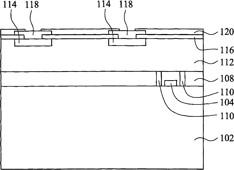
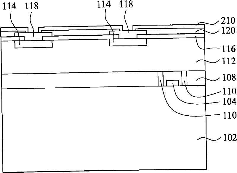
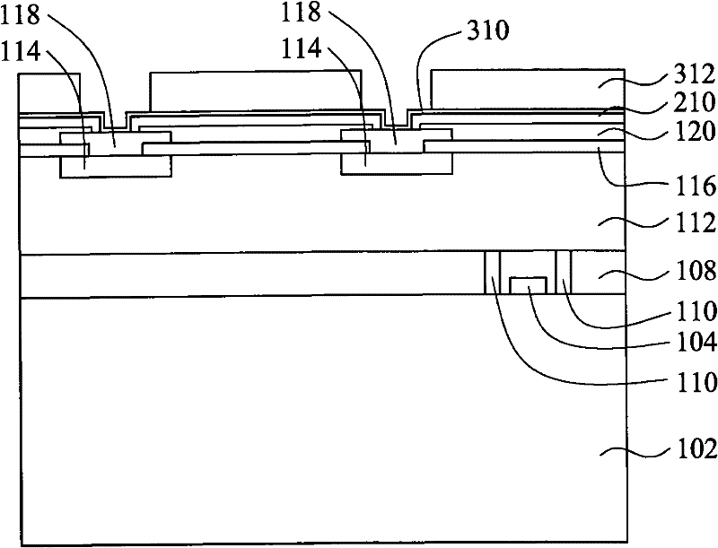
[0026] Embodiments described herein relate to a two-step plasma treatment for polymer surfaces to provide a contaminant-free surface for use in semiconductor devices. As discussed below, embodiments of the present invention disclose the use of a first plasma treatment process from the surface of the substrate to roughen the surface of the polymer layer and loosen the structure of metal contaminants for subsequent etching to remove the contaminants, and using The second plasma treatment process makes the surface smoother, wherein the substrate can be a die, a wafer, a printed circuit board, ...


PUM


Abstract

A semiconductor device having a polymer layer and a method of fabricating the same is provided. A two-step plasma treatment for a surface of the polymer layer includes a first plasma process to roughen the surface of the polymer layer and loosen contaminants, and a second plasma process to make the polymer layer smoother or make the polymer layer less rough. An etch process may be used between the first plasma process and the second plasma process to remove the contaminants loosened by the first plasma process. In an embodiment, the polymer layer exhibits a surface roughness between about 1% and about 8% as measured by Atomic Force Microscopy (AFM) with the index of surface area difference percentage (SADP) and/or has surface contaminants of less than about 1% of Ti, less than about 1% of F, less than about 1.5% Sn, and less than about 0.4% of Pb.

Description

technical field [0001] The present invention relates to a semiconductor device, and in particular to a semiconductor device whose surface is treated with plasma to reduce or avoid contamination. Background technique [0002] Since the advent of the integrated circuit (IC), the semiconductor industry has continued to grow rapidly due to the continuous improvement in the integration of various electronic components (such as transistors, diodes, resistors, capacitors, etc.). Mainly, the improvement of density comes from the continuous reduction of the minimum size of components, so that more components can be integrated into a unit area. [0003] In recent years, it has been seen that many changes in semiconductor packaging have impacted the entire semiconductor industry. Surface-mount technology (SMT) and ball grid array (BGA) packaging are generally important steps for high-throughput packaging of various IC components, and also reduce the pitch of pads on printed circuit bo...

Claims


Application Information

Patent Timeline
IPC IPC(8): H01L23/29H01L21/48
CPCH01L2924/01006H01L2924/01075H01L2924/15311H01L2224/93H01L2924/12044H01L2224/1183H05K3/28H01L2924/01072H01L2924/01084H05K3/3478H01L23/49816H01L2924/01047H01L2224/05624H01L2924/01079H01L23/293H01L2924/01322H01L2924/01013H01L2924/14H01L2924/01078H01L2224/05655H01L24/03H01L2224/1181H05K3/4007H01L2924/01074H01L2224/03452H01L2924/01327H01L23/49822H01L24/11H05K2003/4023H01L2924/01082H01L23/498H01L2224/05644H01L2224/11849H01L2224/0401H01L2224/03462H01L2924/01073H01L24/13H01L2924/01033H01L2224/13116H01L2224/05572H01L2224/03901H01L2224/0362H01L2924/01019H01L2924/1434H01L2224/11622H01L2924/014H01L2224/13111H01L2224/11901H01L2224/05647H01L2224/05639H01L2924/0105H01L2924/01029H01L2224/05669H01L2224/0345H01L24/05H01L23/3171H01L2224/03831H01L2224/1147H01L2924/00014H01L2924/0002H01L2924/15788H01L2924/181H01L2224/11H01L2224/05552H01L2924/00H01L2924/1082
Inventor 卢祯发刘重希余振华陈威宇陈正庭
Owner TAIWAN SEMICON MFG CO LTD
Why Eureka
Try Eureka