A method for improving frequency characteristics of algan/gan HEMT

A technology of frequency characteristics and wet etching, applied in semiconductor/solid-state device manufacturing, semiconductor devices, electrical components, etc., can solve problems affecting device frequency performance, increase, etc., to increase the highest oscillation frequency, increase the cut-off frequency, suppress The effect of the current collapse effect

Inactive Publication Date: 2011-12-28
INST OF MICROELECTRONICS CHINESE ACAD OF SCI
View PDF0 Cites 5 Cited by
  • Summary
  • Abstract
  • Description
  • Claims
  • Application Information

AI Technical Summary

Problems solved by technology

However, the resulting parasitic capacitance between the gate and the dielectric results in a gate-source capacitan

Method used


Image

  • A method for improving frequency characteristics of algan/gan HEMT
  • A method for improving frequency characteristics of algan/gan HEMT
  • A method for improving frequency characteristics of algan/gan HEMT

Examples


Embodiment Construction

[0026] In order to make the object, technical solution and advantages of the present invention clearer, the present invention will be described in further detail below in conjunction with specific embodiments and with reference to the accompanying drawings.

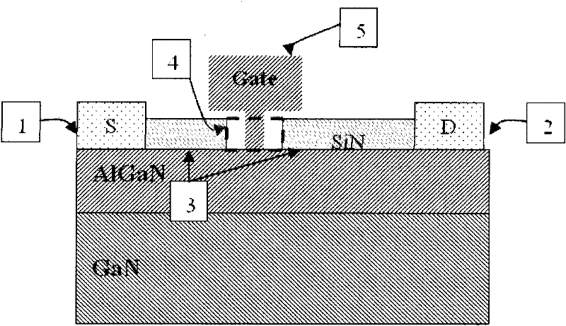
[0027] The present invention can be applied to GaN-based HEMT devices in the millimeter wave and frequency bands above the millimeter wave, and is now combined with figure 1 with figure 2 The present invention is described in detail:

[0028] figure 1 It is a cross-sectional view of a GaN-based HEMT device structure with a conventional structure in the prior art. The formation process includes: forming the source electrode 1 and the drain electrode 2 by rapid annealing alloy; 3 N 4 3, the thickness is 1200 Through ICP etching, the gate groove 4 is formed; through electron beam direct writing, a T-shaped grid 5 is formed, the metal composition of the T-shaped grid is Ni / Au, and the thickness of the T-shaped grid foot...


PUM


Abstract

The invention discloses a method for improving the frequency characteristic of AlGaN/GaN HEMT, which comprises: wiring a millimeter-wave GaN HEMT device with a conventional structure, and then forming a metal protection pattern on the surface of the device by optical lithography; The wet etching process performs a medium corrosion on the device; peels and removes the glue on the etched device. The invention reduces parasitic capacitances of the gate source and the gate drain, and improves the cut-off frequency (ft) and the highest oscillation frequency (fmax) of the device.

Description

technical field [0001] The invention relates to the technical field of structural design of a high electron mobility field effect transistor (HEMT), in particular to a method for improving frequency characteristics of an aluminum gallium nitride / gallium nitride HEMT (AlGaN / GaN HEMT). Background technique [0002] Millimeter-band power amplifiers have great application prospects in military, commercial and consumer fields. High-frequency broadband wireless communication technology, precision guided weapons, long-range radar and space communication technology, the working frequency band is gradually developing from C and X bands to higher frequency bands such as Ku and Ka. [0003] As a third-generation semiconductor material, GaN materials have a wide band gap, high breakdown electric field, and high output power. Because they can work under high voltage and have low on-resistance, GaN devices also show higher gain. At the same time, GaN devices have high electron mobility a...

Claims


Application Information

Patent Timeline
IPC IPC(8): H01L21/335H01L21/311H01L29/778
Inventor 刘果果魏珂黄俊刘新宇
Owner INST OF MICROELECTRONICS CHINESE ACAD OF SCI
Why Eureka
Try Eureka