Method for preparing multistage metal micro-nanostructures inside micro fluidic chip

A technology of microfluidic chips and micro-nano structures, which is applied in the fields of microelectronics and life sciences, and can solve problems such as difficult integration of multi-level metal micro-nano structures

Inactive Publication Date: 2012-01-11
JILIN UNIV
View PDF8 Cites 40 Cited by
  • Summary
  • Abstract
  • Description
  • Claims
  • Application Information

AI Technical Summary

Problems solved by technology

[0008] The purpose of the present invention is to overcome the problem that it is difficult to integrate multi-level metal micro-nano structures on non-planar substrates such as microfluidic chips in the exist

Method used


Image

  • Method for preparing multistage metal micro-nanostructures inside micro fluidic chip
  • Method for preparing multistage metal micro-nanostructures inside micro fluidic chip
  • Method for preparing multistage metal micro-nanostructures inside micro fluidic chip

Examples


Embodiment 1

[0061] Example 1: Preparation of two-dimensional silver micro-nano structures by laser processing on various substrates

[0062] (1) Configure silver plating solution for laser processing

[0063] a. Main salt: Silver nitrate (Silver nitrate, AgNO 3 ; FW 169.88; boiling point 440 ° C; melting point 212 ° C;), the concentration is 0.083mol / L.

[0064] b. Complexing agent: ammonia aqueous (ammonia aqueous), add an appropriate amount to make the silver nitrate solution just clear and slowly add dropwise to adjust the pH value to 10.8.

[0065] c. Reducing agent: sodium gluconate (sodium gluconate, molecular formula: C 6 h 11 NaO 7 , molecular weight 218, content not less than 99.0%, analytically pure, Tianjin Guangfu Institute of Fine Chemicals), concentration 0.078mol / L.

[0066] Configuration process: at room temperature, first weigh 0.034g of silver nitrate and 0.034g of sodium gluconate and mix them directly in a small vial, add 2mL of deionized water, and then dropwise ...

Embodiment 2

[0083] Example 2: Preparation of 3-level silver micro-nano structure by laser processing

[0084] (1) Preparation of silver plating solution for laser processing

[0085] The step of preparing the silver plating solution for laser processing is the same as in Example 1.

[0086] (2) Build micro-nano processing system and design processing program

[0087] With embodiment 1.

[0088] (3) Prepare the substrate for processing

[0089] With embodiment 1.

[0090] (4) Preparation of multi-level silver nanosheet micro-nano structure

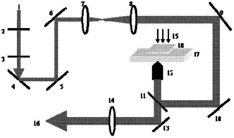
[0091] [1] using figure 1 The processing system shown is to prepare multi-level silver micro-nano structures in the chip channel. The processing program is designed based on the rectangular block structure, and the scanning path is scanned point by point from outside to inside clockwise or counterclockwise or horizontally from left to right. Nanosheet silver microstructures were prepared by controlling the scanning step length, the number of sca...

Embodiment 3

[0105] Example 3: Local and selective integration of SERS detection substrates in microfluidic chips

[0106] (1) Preparation of silver plating solution for laser processing

[0107] The step of preparing the silver plating solution for laser processing is the same as in Example 1.

[0108] (2) Build micro-nano processing system and design processing program

[0109] With embodiment 1.

[0110] (3) Prepare the chip

[0111] The microfluidic chip to be used is subjected to routine cleaning treatment, ultrasonic cleaning with acetone, ethanol, and deionized water.

[0112] (4) Preparation of multi-level silver micro-nano structures at the bottom of the chip channel

[0113] Pack the plating solution in the channel of the microfluidic chip with an air pump, place the chip in the laser processing system, and use the three-dimensional mobile platform and monitoring system to find the specific position in the channel where the silver micro-nano structure is to be integrated, and...


PUM

PropertyMeasurementUnit
Boiling pointaaaaaaaaaa
Melting pointaaaaaaaaaa
Spot diameteraaaaaaaaaa

Abstract

The invention relates to a method for selectively preparing or integrating multistage silver micro-nanostructures inside various plane substrates and micro fluidic chip channels by the utilization of the femtosecond laser inducing metallic silver reduction technology. In addition, the silver multistage micro-nanostructure substrate prepared by the method is used as a reinforced substrate for surface-enhanced raman spectroscopy SERS. The method provided by the invention comprises the following steps of: preparing a silver plating solution for femtosecond laser micro-nano machining, establishing a femtosecond laser micro-nano machining system for realizing multi-point scan in the silver plating solution, placing the silver plating solution and the substrate into the femtosecond laser micro-nano machining system and preparing the multistage silver micro-nanostructures on the substrate. According to the invention, a laser beam scans in the silver plating solution along a track designed in advance by a program. The preparation method is independent of the smoothness of the substrate. In particular, the preparation of silver multistage structure SERS substrate can be accomplished on the bottom of the micro fluidic chip channels, thus realizing catalysis and surface-enhanced raman test application.

Description

technical field [0001] The invention belongs to the technical field of microelectronics and life sciences, and specifically relates to a femtosecond laser-induced metal silver reduction technology to selectively prepare or integrate metal silver on various planar substrates and non-planar substrates such as microfluidic chip channels. approach to micro-nanostructures. Background technique [0002] Microfluidics, also known as biochip technology, integrates the basic operation units of sample preparation, reaction, separation, and detection in the process of biological, chemical, and medical analysis into a micron-scale chip to automatically complete the entire analysis process. . Due to its great potential in the fields of biology, chemistry, and medicine, this technology has developed into a new research field interdisciplinary in biology, chemistry, medicine, fluid, electronics, materials, and machinery. The microfluidic chip has the characteristics of controllable liqui...

Claims


Application Information

Patent Timeline
IPC IPC(8): B81C1/00
Inventor 徐彬彬孙洪波夏虹陈岐岱张永来
Owner JILIN UNIV
Why Eureka
Try Eureka