Integrated circuit parallel testing method, device and system

A technology for judging circuits and output circuits, applied in the field of integrated circuits, which can solve the problems of limited test channels, test efficiency, and inability to achieve large-scale simultaneous/parallel comparison of units under test.

Active Publication Date: 2012-01-11
SHANGHAI XINHAO MICROELECTRONICS
View PDF6 Cites 20 Cited by
  • Summary
  • Abstract
  • Description
  • Claims
  • Application Information

AI Technical Summary

Problems solved by technology

[0013] To sum up, the existing integrated circuit testing methods, devices and systems, due to the limitation of the number of test channels, can only test one or several units under test at a time, and cannot achieve large-scale simultaneous / parallel comparison of the units under test.
The limited number of test channels is the bottleneck restricting the improvement of test efficiency

Method used


Image

  • Integrated circuit parallel testing method, device and system
  • Integrated circuit parallel testing method, device and system
  • Integrated circuit parallel testing method, device and system

Examples


Embodiment Construction
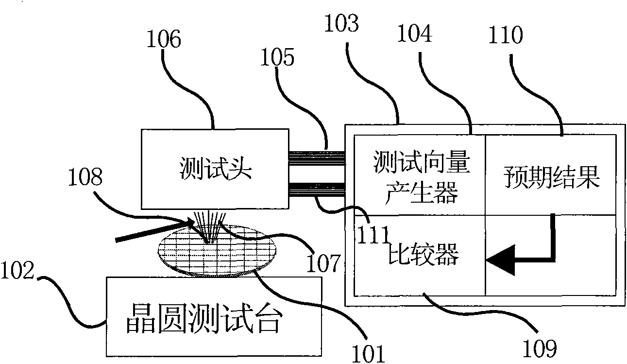
[0160] The technical idea of ​​the present invention is that a plurality of tested integrated circuits / chips / functional chips with the same structure and function execute the same input stimulus, each of which produces operation results, and the operation results are compared with each other or with the expected results in parallel to detect failures Integrated circuit / die / functional chip.

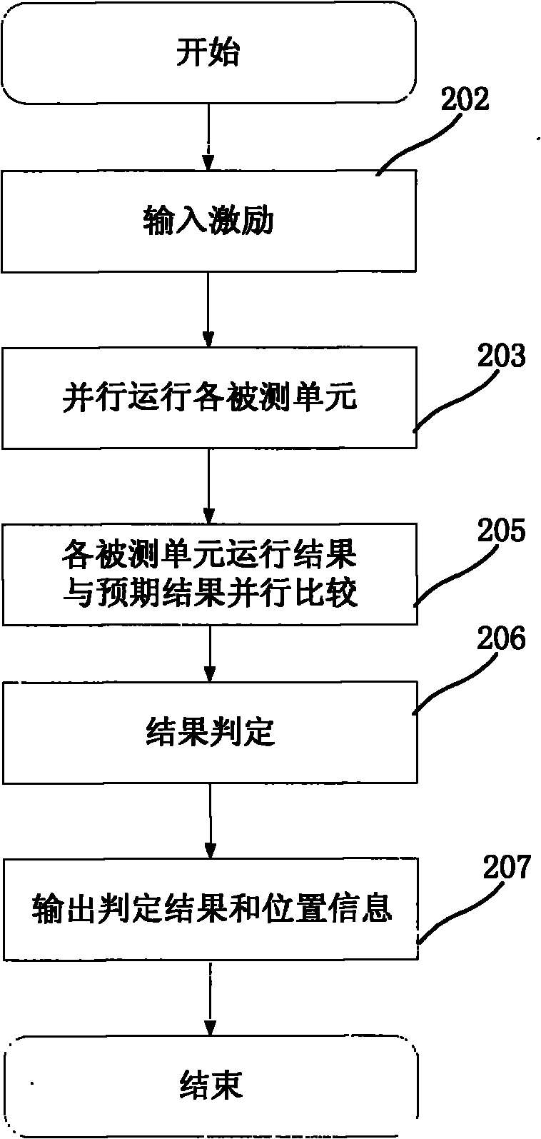
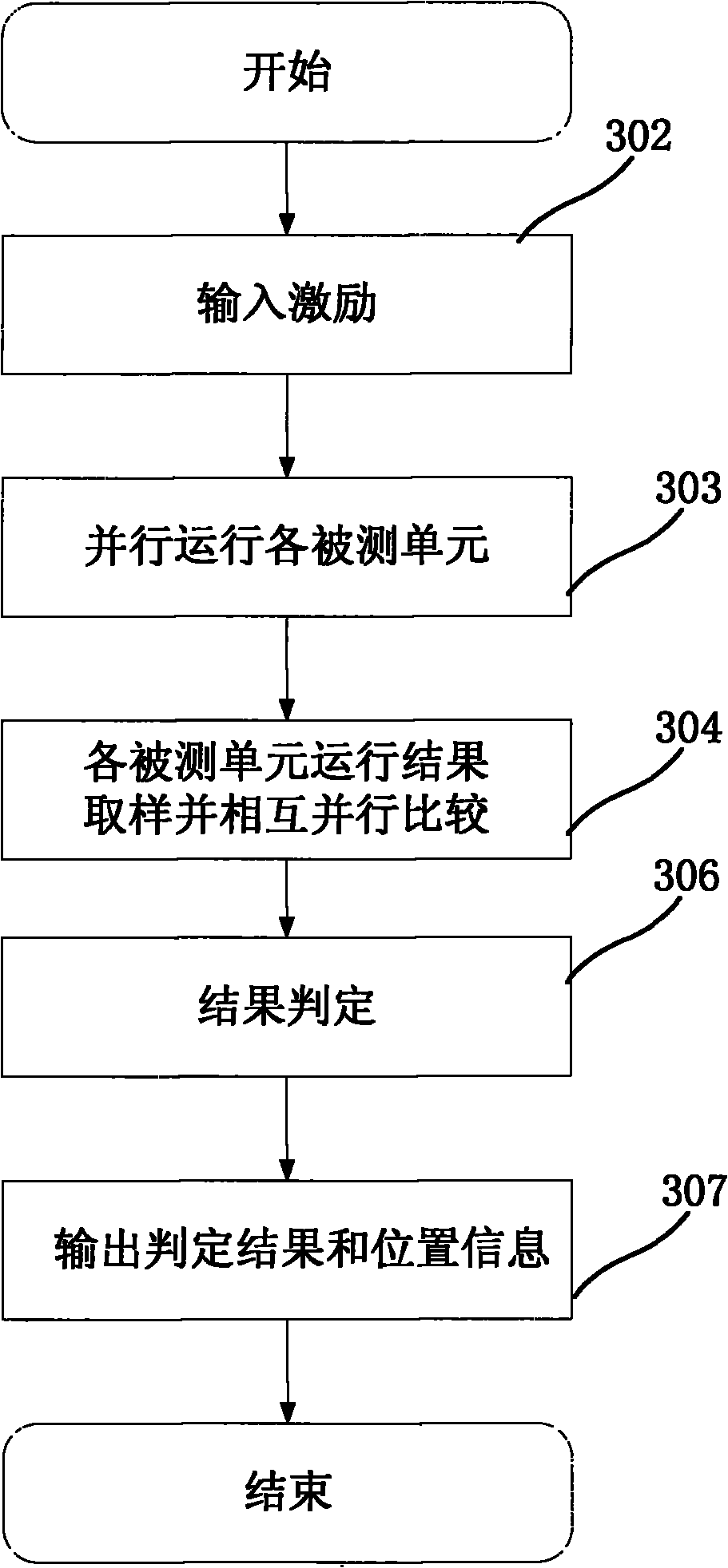
[0161] see figure 2 , figure 2 It is a flow chart of testing under the condition that the common substrate integrated circuit testing device of the present invention has expected results. The comparison device in this embodiment does not include a failure judgment function. First enter step one (202), input excitation, and then enter step two (203) to run each unit under test in parallel. Then enter step 3 (205) to sample the operation results of each unit under test, and compare them in parallel with the expected results, and record the comparison results. The number of sampling comp...


PUM


Abstract

The invention discloses an integrated circuit testing method, device and system. A common substrate comprises a plurality of units to be tested and a plurality of operation result comparison devices for the units to be tested, wherein different units to be tested execute same input excitation and generate respective operation results, the operation results are compared by the corresponding operation result comparison devices to generate comparison features, and invalid tested units are detected according to the features. According to the invention, the testing cost can be reduced, the time for forming scale mass production can be shortened, and the missing rate is decreased.

Description

technical field [0001] The invention belongs to the field of integrated circuits, in particular to a parallel testing method, device and system for integrated circuits. Background technique [0002] A typical semiconductor fabrication process is to fabricate multiple identical rectangular dies on a thin, uniform wafer of semiconductor material. The grains are separated by scribe lines with a width of 60-80 microns. Mask alignment marks and wafer acceptance test (WAT) test elements are often placed on the dicing lanes to monitor quality during production. [0003] During the manufacturing process, the photolithography machine exposes one area at a time, called a stepper field, and each photolithography area contains one or more crystal grains. When all fabrication steps are complete, each die on the wafer must pass functional testing. Wafer test equipment (wafer prober) uses a probe card to contact the pad of the die to be tested, and transmits the test stimulus generated ...

Claims


Application Information

Patent Timeline
Patent Type & Authority Applications(China)
IPC IPC(8): G01R31/303
Inventor 林正浩
Owner SHANGHAI XINHAO MICROELECTRONICS
Why Eureka
Try Eureka