Schottky barrier metal oxide semiconductor (MOS) transistor and preparation method thereof

A technology of MOS transistor and Schottky potential, which is applied in the field of Schottky barrier MOS transistor and its preparation, can solve the problems of large conduction current and large conduction current of devices, and achieve the improvement of conduction current and open state Effect of current and low parasitic resistance

Active Publication Date: 2012-01-18
SEMICONDUCTOR MANUFACTURING INTERNATIONAL (BEIJING) CORP +1
View PDF2 Cites 6 Cited by
  • Summary
  • Abstract
  • Description
  • Claims
  • Application Information

AI Technical Summary

Problems solved by technology

First of all, since the on-state current mainly comes from the tunneling of the source carrier, the on-state current is limited, and the small on-state current becomes one of the main reasons for limiting the application of SB-MOSFET; secondly, SB-MOSFET has a serious bipolar effect, that is, when the gate is reverse-biased, the device will also generate a large conduction current, so that the gate will appear when a certain forward and reverse bias is applied. Large conduction current

Method used


Image

  • Schottky barrier metal oxide semiconductor (MOS) transistor and preparation method thereof
  • Schottky barrier metal oxide semiconductor (MOS) transistor and preparation method thereof
  • Schottky barrier metal oxide semiconductor (MOS) transistor and preparation method thereof

Examples


Embodiment 1

[0044] Adopt the following method to prepare the MOS transistor of the present invention:

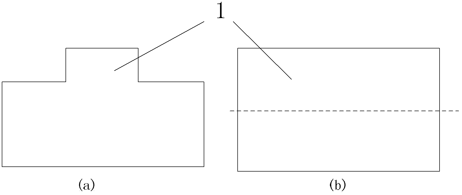
[0045] (1) On the bulk silicon wafer silicon substrate 1 with the crystal orientation of (100), the shallow trench isolation technology is used to fabricate the active region isolation layer, and the doping concentration of the substrate is N-type lightly doped; then, a step pattern is formed by photolithography , etch a step structure, the step height is about 500nm, such as figure 1 (a), 1(b);

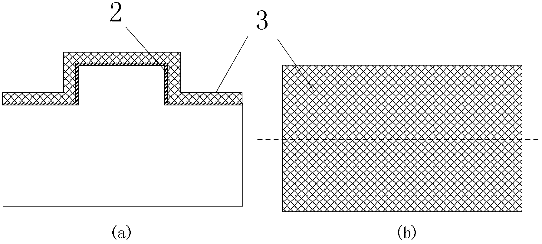
[0046] (2) thermally grow the gate dielectric layer, and then deposit the gate electrode layer, the gate dielectric layer is SiO 2 , the thickness is 1-5nm, the gate electrode layer is a highly doped polysilicon layer, the thickness is about 200nm, such as figure 2 (a), as shown in 2(b);

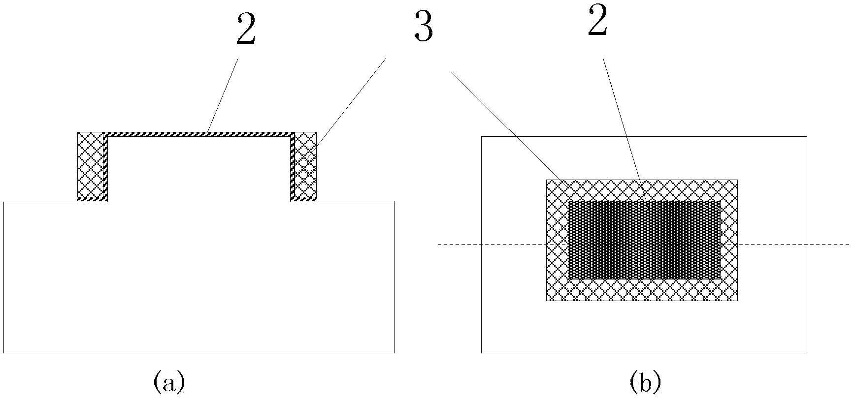
[0047] (3) The ring-shaped gate electrode 3 is formed by using the sidewall process, and the thickness of the gate electrode is about 200nm, such as image 3 (a), 3(b);

[0048] (4) Deposit the side wa...

Embodiment 2

[0053] As in Example 1, the difference is:

[0054] The step height in step (1) is about 200nm;

[0055] The thickness of the gate electrode in steps (2) and (3) is about 100nm;

[0056] The thickness of the sidewall in steps (4) and (5) is about 50nm;

[0057] ●The sputtered metal in step (6) is a metal with a smaller hole Schottky barrier, such as Pt.

Embodiment 3

[0059] As in Example 1, the difference is:

[0060] The substrate doping in step (1) is P-type lightly doped;

[0061] ●The sputtered metal in step (6) is a metal with a small electronic Schottky barrier, such as rare earth metal Er or Yb.


PUM


Abstract

The invention discloses a Schottky barrier metal oxide semiconductor (MOS) transistor, which comprises a ring-shaped gate electrode (3), a ring-shaped gate dielectric layer (2), a ring-shaped gate electrode side wall (4), a semiconductor substrate, a source region (5) and a ring-shaped drain region (6). The Schottky barrier MOS transistor is characterized in that: the semiconductor substrate is provided with a convex step structure; the source region is positioned on a high plane of a convex step; the ring-shaped drain region surrounds the convex step and is positioned on a low plane; the gate dielectric layer and the gate electrode are positioned at a corner of the convex step, surrounds the step and is raised into a ring shape; and the gate electrode side wall is ring-shaped, surrounds on the outer side of the gate electrode and has a certain thickness to serve as a shelter to form an underlap structure of a drain terminal. The Schottky barrier MOS transistor adopts a step structurecombining a ring-shaped gate structure and an asymmetric source / drain structure, so on the basis of inheriting advantages of traditional SB-MOSFET, the on-state conduction current is improved, a dipolar effect is inhibited, and the process is simplified.

Description

technical field [0001] The invention belongs to the field of field effect transistor logic devices and circuits in CMOS ultra-large integrated circuits (ULSI), and specifically relates to a Schottky barrier MOS transistor combined with a step structure, a ring gate structure and an asymmetric source / drain structure and its preparation method. Background technique [0002] As early as the late 1960s, Lepselter and Sze proposed the Schottky Barrier MOSFET (Schottky Barrier MOSFET) structure. The source and drain are replaced with metal or silicide for traditional doping, and the direct tunneling barrier of carriers at the source end is used to achieve conduction. As the size of metal-oxide-silicon field-effect transistors (MOSFETs) continues to shrink, short-channel effects are increasingly affecting the devices. For traditional MOS field effect transistors, in order to suppress the short-channel effect, ultra-shallow junctions and abruptly doped source / drain regions must be...

Claims


Application Information

Patent Timeline
Patent Type & Authority Applications(China)
IPC IPC(8): H01L29/10H01L29/423H01L29/78H01L21/28H01L21/336
Inventor 黄如江文哲黄芊芊詹瞻邱颖鑫
Owner SEMICONDUCTOR MANUFACTURING INTERNATIONAL (BEIJING) CORP
Why Eureka
Try Eureka