
Enhancement of organic photovoltaic cell open circuit voltage using electron/hole blocking exciton blocking layers

A technology of electron blocking layer and hole blocking layer, applied in the field of photosensitive optoelectronic devices

Inactive Publication Date: 2012-01-25
RGT UNIV OF MICHIGAN
View PDF5 Cites 19 Cited by
  • Summary
  • Abstract
  • Description
  • Claims
  • Application Information

AI Technical Summary

Problems solved by technology

However, long-wavelength absorbing materials such as SnPc generally result in low V OC battery

Method used


Image

  • Enhancement of organic photovoltaic cell open circuit voltage using electron/hole blocking exciton blocking layers
  • Enhancement of organic photovoltaic cell open circuit voltage using electron/hole blocking exciton blocking layers
  • Enhancement of organic photovoltaic cell open circuit voltage using electron/hole blocking exciton blocking layers

Examples


Embodiment 1

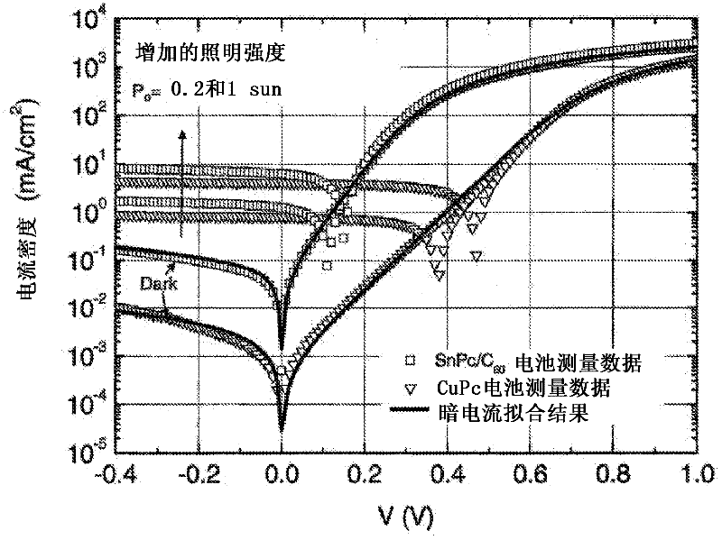
[0113] pre-coated on glass substrates Thick ITO layer (15Ω / cm 2 The device is fabricated on the sheet resistance). The solvent-cleaned ITO surface was exposed to UV / O 3 - for 5 minutes and then immediately loaded it into a high vacuum chamber (base pressure -7 Torr), in which the organic layers are sequentially deposited by thermal evaporation and Thick Al cathode. The deposition rate of the purified organic layer is (Laudise et al., J Cryst. Growth, 187, 449 (1998)). An Al cathode was evaporated through a mask with a 1 mm diameter opening to define the active area of ​​the device. Current density vs. voltage (J-V) characteristics were measured under dark conditions and under simulated AM1.5G solar illumination. Illumination intensity and quantum efficiency measurements were performed using a NREL calibrated Si detector using standard methods (ASTM Standards E1021, E948 and E973, 1998).

[0114] figure 1 ITO / SnPc is shown / C60 / Bath Copper Spirit (BCP, ) / Al ...

Embodiment 2

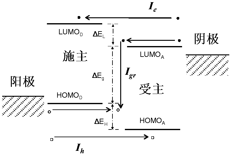
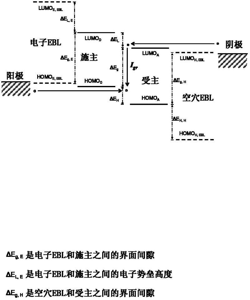
[0117] In SnPc / C 60 battery, in order to reduce the J S , and thus increasing V OC , an electron blocking EBL was inserted between the anode and the SnPc donor layer described in Example 1. According to the energy level diagram in the inset of Fig. 2, the electron-blocking EBL should (i) have a higher LUMO energy than the donor LUMO, (ii) have a relatively high hole mobility, and (iii) confine Dark current due to generation and recombination at , due to small electron blocking EBL (LUMO) to donor (LUMO) "interfacial gap" energy. According to these considerations, the inorganic material MoO 3 And subphthalocyanine borochloride (SubPc) and CuPc are used as electron blocking EBL (Mutolo et al., J. Am. Chem. Soc, 128, 8108 (2006)). According to their respective energy levels (Fig. 2), they all effectively block the electron current from the donor to the anode contact. MoO has been used before in polymer PV cells 3 To prevent the reaction between ITO and the polymer PV active...


PUM


Abstract

The present disclosure relates to photosensitive optoelectronic devices comprising at least one of an electron blocking or hole blocking layer. Further disclosed are methods of increasing power conversion efficiency in photosensitive optoelectronic devices using at least one of an electron blocking or hole blocking layer. The electron blocking and hole blocking layers presently disclosed may reduce electron leakage current by reducing the dark current components of photovoltaic cells. This work demonstrates the importance of reducing dark current to improve power conversion efficiency of photovoltaic cells.

Description

[0001] Cross References to Related Applications [0002] This application claims priority to US Provisional Application 61 / 144,043, filed January 12, 2009, which is hereby incorporated by reference in its entirety. [0003] Statement Regarding Federally Sponsored Research [0004] This invention was made with US Government support under FA9550-07-1-0364 awarded by the US Air Force Office of Scientific Research and DE-FG36-08GO18022 awarded by the US Department of Energy. The government has certain rights in this invention. [0005] joint research agreement [0006] The claimed invention was made by, on behalf of, and / or in association with one or more of the following parties under a joint university-corporate research agreement: The University of Michigan and Global Photonic Energy Corporation. This agreement was in effect on and before the date this invention was made, and the claimed invention was made as a result of actions taken within the scope of this agreement. ...

Claims


Application Information

Patent Timeline
Patent Type & Authority Applications(China)
IPC IPC(8): H01L51/42H01L51/00
CPCB82Y10/00H01L51/424H01L51/0048Y02E10/549H10K85/221H10K30/20H10K30/50H10K30/30H10K30/353H10K85/211H10K30/81H10K30/00H10K85/324H10K85/311H10K85/623H10K85/621H10K85/342H10K85/40H10K85/60H10K85/381
Inventor 史蒂芬·R·福里斯特李宁
Owner RGT UNIV OF MICHIGAN
Learn More