Light-emitting diode epitaxial wafer and preparation method thereof

A technology of light-emitting diodes and epitaxial wafers, which is applied in the direction of electrical components, circuits, semiconductor devices, etc., can solve problems such as lattice mismatch and product yield decline, and achieve improved crystal quality, product yield, and antistatic ability Effect

Inactive Publication Date: 2016-07-06
HC SEMITEK SUZHOU
View PDF3 Cites 36 Cited by
  • Summary
  • Abstract
  • Description
  • Claims
  • Application Information

AI Technical Summary

Problems solved by technology

[0006] In order to solve the problems of lattice mismatch and product yield drop in the prior art, the emb

Method used


Image

  • Light-emitting diode epitaxial wafer and preparation method thereof
  • Light-emitting diode epitaxial wafer and preparation method thereof

Examples


Embodiment 1

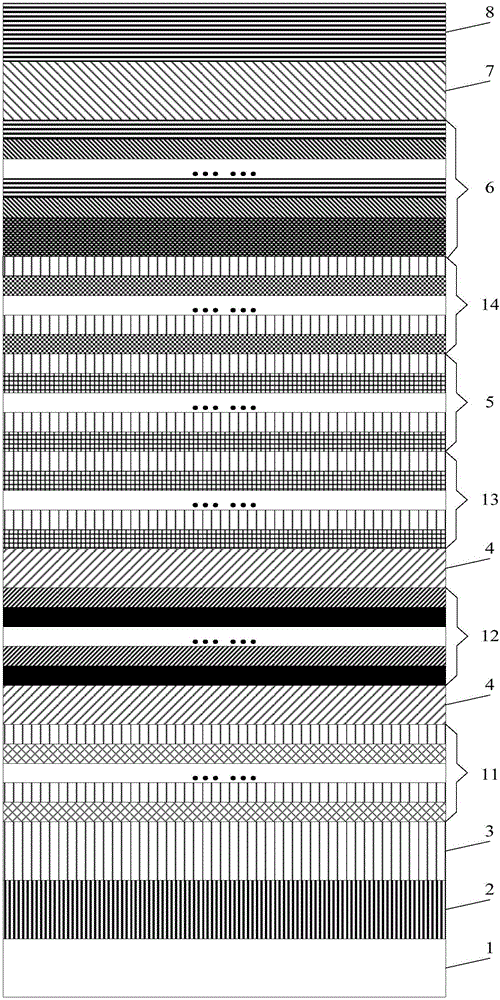
[0033] An embodiment of the present invention provides a light emitting diode epitaxial wafer, see figure 1 , the light-emitting diode epitaxial wafer includes a sapphire substrate 1, and a low-temperature buffer layer 2, a high-temperature non-doped GaN layer 3, an N-type GAN layer 4, a multi-quantum well layer 5, and a P-type electronic layer sequentially stacked on the sapphire substrate 1. Barrier layer 6, P-type GAN layer 7, P-type contact layer 8, the light-emitting diode epitaxial wafer also includes a first defect barrier layer 11 arranged between the high-temperature non-doped GaN layer 3 and the N-type GAN layer 4, inserted in the The second defect barrier layer 12 in the N-type GAN layer 4, the stress release layer 13 arranged between the N-type GAN layer 4 and the multi-quantum well layer 5, the first defect barrier layer 11 includes alternately stacked AlGaN layers and GaN layers , the second defect barrier layer 12 includes alternately stacked SiN film layers and...

Embodiment 2

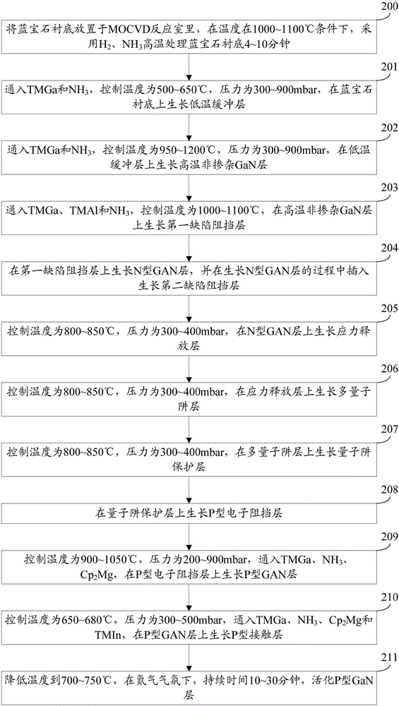
[0078] The embodiment of the present invention provides a method for preparing a light-emitting diode epitaxial wafer, see figure 2 , the preparation method comprises:

[0079] Step 200: Place the sapphire substrate in a Metal-organic Chemical Vapor Deposition (MOCVD) reaction chamber, and use H 2 , NH 3 Treat the sapphire substrate at high temperature for 4-10 minutes.

[0080] Step 201: Passing TMGa and NH 3 , the temperature is controlled at 500-650° C., the pressure is 300-900 mbar, and a low-temperature buffer layer is grown on the sapphire substrate.

[0081] Optionally, the low-temperature buffer layer may be a GaN layer or an AlGaN layer.

[0082] Optionally, the thickness of the low-temperature buffer layer may be 20-50 nm.

[0083] Preferably, after step 201, the preparation method may further include:

[0084]Raise the temperature to 950-1100° C., anneal at a high temperature for 60-300 s, and the low-temperature buffer layer becomes a GaN crystal nucleus.

...


PUM

PropertyMeasurementUnit
Thicknessaaaaaaaaaa
Thicknessaaaaaaaaaa
Thicknessaaaaaaaaaa

Abstract

The invention discloses a light-emitting diode epitaxial wafer and a preparation method thereof, and belongs to the technical field of semiconductors. The light-emitting diode epitaxial wafer comprises a sapphire substrate, a low-temperature buffer layer, a high-temperature non-doped GaN layer, a first defect barrier layer, an N-type GaN layer, a stress release layer, a multi-quantum well layer, a P-type electron blocking layer, a P-type GaN layer and a P-type contact layer, wherein the low-temperature buffer layer, the high-temperature non-doped GaN layer, the first defect barrier layer, the N-type GaN layer, the stress release layer, the multi-quantum well layer, the P-type electron blocking layer, the P-type GaN layer and the P-type contact layer are sequentially laminated on the sapphire substrate; a second defect barrier layer is inserted into the N-type GaN layer; the first defect barrier layer comprises alternately laminated AlGaN layers and GaN layers; the second defect barrier layer comprises alternately laminated SiN films and N-type AlGaN layers; and the stress release layer comprises alternately laminated InGaN layers and GaN layers. According to the light-emitting diode epitaxial wafer, extension of defects formed by lattice mismatch into the multi-quantum well layer is effectively suppressed; stress release is enhanced; the crystal quality is improved; leakage passages are reduced; the anti-static electricity capacity of an LED chip is improved; and the product yield is improved.

Description

technical field [0001] The invention relates to the technical field of semiconductors, in particular to a light-emitting diode epitaxial wafer and a preparation method thereof. Background technique [0002] Light Emitting Diode (LED for short) is a semiconductor electronic component that can emit light. Gallium nitride-based materials have excellent properties such as wide direct bandgap, strong chemical bonds, high temperature resistance, and corrosion resistance. They are ideal materials for the production of short-wavelength high-brightness light-emitting devices, ultraviolet light detectors, and high-temperature and high-frequency microelectronic devices. Full-color large-screen display, LCD backlight, signal lights, lighting and other fields. [0003] The existing LED epitaxial wafer includes a substrate, and a low-temperature buffer layer, a high-temperature non-doped GaN layer, an N-type layer, a multi-quantum well layer, a P-type electron blocking layer, a P-type la...

Claims


Application Information

Patent Timeline
IPC IPC(8): H01L33/06H01L33/12H01L33/32H01L33/00
CPCH01L33/06H01L33/0066H01L33/0075H01L33/12H01L33/32
Inventor 马欢田艳红周飚胡加辉魏世祯
Owner HC SEMITEK SUZHOU
Why Eureka
Try Eureka