Gallium-nitride-based light emitting diode capable of improving electron injection efficiency

A light-emitting diode and electron injection technology, which is applied in circuits, electrical components, semiconductor devices, etc., can solve problems such as the increase of Fermi energy level and the aggravation of electronic overshoot behavior

Active Publication Date: 2011-09-14
INST OF SEMICONDUCTORS - CHINESE ACAD OF SCI
View PDF6 Cites 34 Cited by
  • Summary
  • Abstract
  • Description
  • Claims
  • Application Information

AI Technical Summary

Problems solved by technology

However, with the increase of the injected current density, since the applied electric field is in the same direction as the compressive strain electric field in the active layer, the Fermi energy level in the n region is further increased, and the overshoot behavior of electrons is aggravated, and a large number of electrons still cross the active layer. directly to the p zone

Method used


Image

  • Gallium-nitride-based light emitting diode capable of improving electron injection efficiency
  • Gallium-nitride-based light emitting diode capable of improving electron injection efficiency
  • Gallium-nitride-based light emitting diode capable of improving electron injection efficiency

Examples


Embodiment Construction

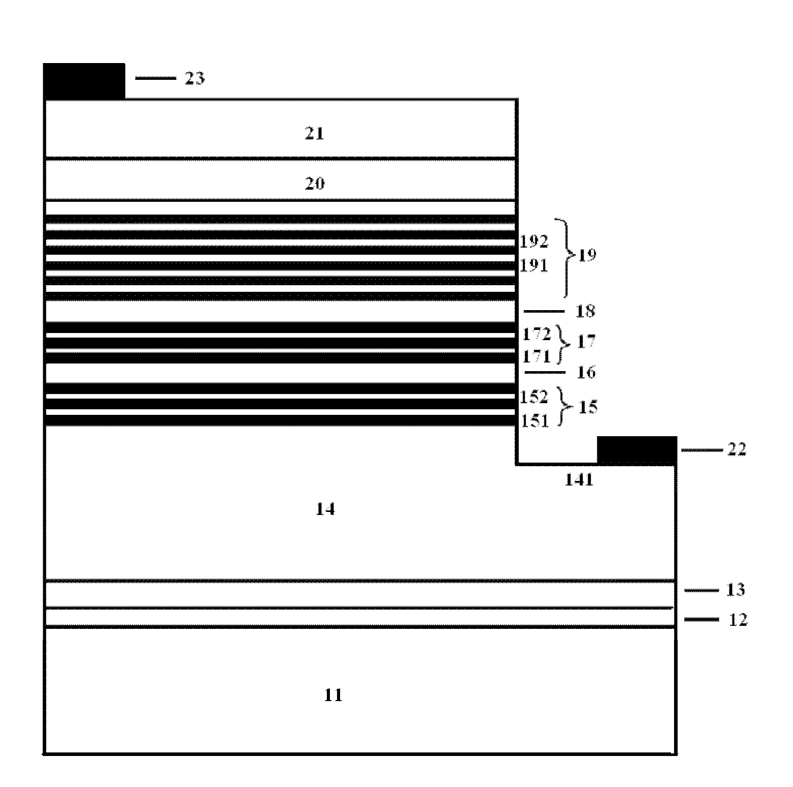
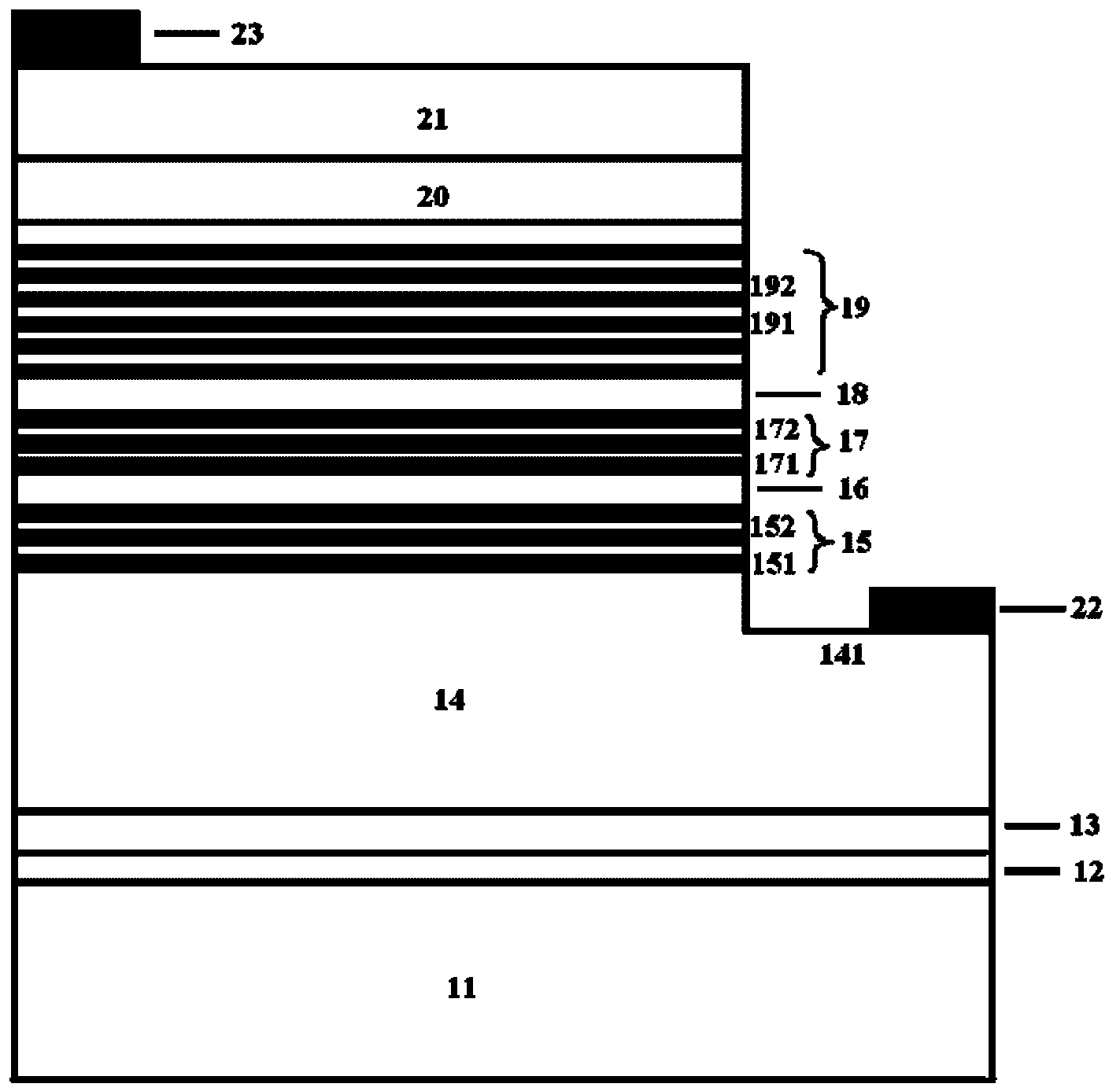
[0023] see figure 1 As shown, the present invention provides a gallium nitride-based light-emitting diode, which includes:

[0024] A substrate 11, from (0001) to sapphire (Al 2 o 3 ) is the substrate 11, and other materials that can be used for the substrate 11 also include aluminum oxide single crystals on the R-plane or A-plane, 6H-SiC, 4H-SiC, or single crystal oxides whose lattice constants are close to those of nitride semiconductors thing. High-purity NH was used in the preparation 3 As N source, high-purity H 2 and N 2 mixed gas as carrier gas; trimethylgallium or triethylgallium as Ga source, trimethylindium as In source, trimethylaluminum as Al source; n-type dopant is silane, p-type dopant is Magnesium dichloride.

[0025] A gallium nitride nucleation layer 12 , the gallium nitride nucleation layer 12 is fabricated on the substrate 11 . Growth parameters include: reaction temperature 500°C to 800°C, reaction chamber pressure 200 to 500 Torr, carrier gas flow...


PUM


Abstract

The invention discloses a gallium-nitride-based light emitting diode capable of improving electron injection efficiency. The gallium-nitride-based light emitting diode comprises a substrate, a gallium nitride nucleation layer, a buffer layer, an n-type contact layer, a lower multicycle n-type electron coupling layer, a lower tunneling potential barrier layer, an upper multicycle n-type electron coupling layer, an upper tunneling potential barrier layer, a multicycle active luminous layer, a negative electrode, a p-type electron blocking layer, a p-type contact layer and a positive electrode, wherein the gallium nitride nucleation layer is manufactured on the substrate; the buffer layer is manufactured on the gallium nitride nucleation layer; the n-type contact layer is manufactured on the buffer layer; a table top is formed on one side of the upper surface of the n-type contact layer; the lower multicycle n-type electron coupling layer is manufactured on the other side of the table top on the n-type contact layer; the lower tunneling potential barrier layer is manufactured on the lower multicycle n-type electron coupling layer; the upper multicycle n-type electron coupling layer is manufactured on the lower tunneling potential barrier layer; the upper tunneling potential barrier layer is manufactured on the upper multicycle n-type electron coupling layer; the multicycle active luminous layer is manufactured on the upper tunneling potential barrier layer; the negative electrode is manufactured on the table top of the n-type contact layer; the p-type electron blocking layer is manufactured on the multicycle active luminous layer; the p-type contact layer is manufactured on the p-type electron blocking layer; and the positive electrode is manufactured on the p-type contact layer to form the structure of the gallium-nitride-based light emitting diode.

Description

technical field [0001] The invention relates to a gallium nitride (GaN) light-emitting diode, in particular to a gallium nitride light-emitting diode with two or more n-type electron coupling layers of different indium components. Background technique [0002] At present, III-V semiconductor optoelectronic materials are known as the third generation semiconductor materials. GaN-based light-emitting diodes have become the focus of industry research because they can produce light-emitting diodes (referred to as "LEDs") of various colors (especially blue or violet light that requires a high energy gap) by controlling the composition of materials. [0003] The epitaxial growth of GaN-based semiconductor materials or devices currently mainly adopts MOCVD technology. In the process of growing nitride semiconductors (GaN, AlN, InN and their alloy nitrides) using MOCVD technology, sapphire is usually used as the substrate for heteroepitaxy because there is no substrate material tha...

Claims


Application Information

Patent Timeline
Patent Type & Authority Applications(China)
IPC IPC(8): H01L33/02H01L33/14H01L33/04
Inventor 马平王军喜魏学成曾一平李晋闽
Owner INST OF SEMICONDUCTORS - CHINESE ACAD OF SCI
Why Eureka
Try Eureka