Nitride light-emitting diode (LED) epitaxial wafer and growing method thereof

A technology of LED epitaxial wafers and growth methods, which is applied in the direction of electrical components, circuits, semiconductor devices, etc., can solve the problems of reduced radiation recombination efficiency, reduced radiation recombination probability, poor antistatic properties, etc., to achieve ESD improvement, reasonable process, The effect of reducing the polarizing electric field

Inactive Publication Date: 2013-03-13
YANGZHOU ZHONGKE SEMICON LIGHTING
View PDF4 Cites 33 Cited by
  • Summary
  • Abstract
  • Description
  • Claims
  • Application Information

AI Technical Summary

Problems solved by technology

[0003] One of the main problems is the reduced radiative recombination efficiency due to stress fields caused by lattice mismatch in InGaN / GaN MQWs
The stress field caused by lattice mismatch in InGaN / GaN multi-quantum well MQWs makes the energy bands in MQWs tilt, resulting in the spatial separation of electron and hole wave functions, thereby reducing the probability of radiative recombination and reducing the luminous brightness.
At the same time, these stress fields cause the LED chip to be easily broken down due to static electricity, that is, the antistatic ability is poor.
[0004] On the other hand, increasing the current spreading efficiency in the current LED structure design is an important way to improve the brightness, but the current spreading layer is generally designed on the chip, the process is complicated and the cost is increased.

Method used


Image

  • Nitride light-emitting diode (LED) epitaxial wafer and growing method thereof

Examples


Embodiment Construction

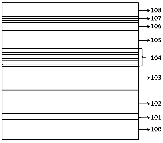
[0019] The growth process adopts MOCVD equipment (Crius 31-piece commercial machine of Aixtron Company), and the V group source used is ammonia gas (NH 3 ), the Group III organic source materials are trimethylgallium (TMGa) and trimethylindium (TMIn), and the P-type and N-type doped well elements are respectively Mg and Si. The substrate can be selected from sapphire, silicon, silicon carbide or gallium arsenide.

[0020] combine figure 1 , the growth step:

[0021] 1. A GaN low-temperature buffer layer 101 with a thickness of 0.01-1 μm is grown on the substrate 100, with H 2 As a carrier gas, the growth temperature is 500-600° C., and the pressure is 50-1000 mbar. In this case the thickness is 30 nm.

[0022] 2. Raise the temperature, grow an unintentionally doped GaN layer 102 with a thickness of about 2 μm on the GaN low-temperature buffer layer 101 under the conditions of a temperature of 800-1200° C. and a pressure of 50-1000 mbar.

[0023] 3. Reheating, on the unint...


PUM


Abstract

The invention provides a nitride light-emitting diode (LED) epitaxial wafer and a growing method thereof and relates to the technical field of semiconductor optoelectronics. The nitride LED epitaxial wafer structurally and sequentially comprises a substrate, a low-temperature buffer layer, an unintentionally doped GaN, an N-shaped electron-injection layer, an InGaN/GaN inserting layer, an active area, an electron blocking layer, a u-GaN/p-GaN superlattice and a p-GaN hole-injection layer from bottom to top. The InGaN/GaN inserting layer is grown between the N-shaped electron-injection layer and the active area so as to effective relieve stress of the active area, lower polarization electric fields, reduce limitation of stark effect through a quantum well, and improve luminance and anti-static properties. The u-GaN/p-GaN superlattice is inserted between the electron blocking layer and the P-shaped hole-injection layer so as to improve current expansion capacity and lower chip operating voltage.

Description

technical field [0001] The invention belongs to the technical field of semiconductor optoelectronics, in particular to the technical field of production of a nitride LED epitaxial wafer. Background technique [0002] Nitride LED as a solid-state light source has the advantages of high efficiency, long life, and environmental protection. It is known as the second revolution in the history of human lighting after Edison invented the electric light, and has become the focus of international semiconductor and lighting research and development and industry attention. However, obtaining high-brightness GaN-based LEDs still faces many technical difficulties. [0003] One of the main problems is the reduced radiative recombination efficiency caused by the stress field caused by lattice mismatch in InGaN / GaN MQWs. The stress field caused by lattice mismatch in InGaN / GaN multi-quantum well MQWs makes the energy bands in MQWs tilt, resulting in spatial separation of electron and hole ...

Claims


Application Information

Patent Timeline
Patent Type & Authority Applications(China)
IPC IPC(8): H01L33/06H01L33/00
Inventor 李鸿渐李盼盼李志聪李璟王国宏
Owner YANGZHOU ZHONGKE SEMICON LIGHTING
Why Eureka
Try Eureka