
One-dimensional axial type nano zinc oxide / zinc sulfide heterojunction and preparation method thereof

A technology of nano-zinc oxide and nano-zinc sulfide, applied in the field of nano-materials, can solve the problems of inability to prepare one-dimensional axial zinc oxide/zinc sulfide heterojunction, limited performance and application, insufficient preparation methods, etc., and achieve cost Low cost, scientific preparation method, uniform product appearance

Inactive Publication Date: 2012-02-08
HEFEI INSTITUTES OF PHYSICAL SCIENCE - CHINESE ACAD OF SCI
View PDF4 Cites 7 Cited by
  • Summary
  • Abstract
  • Description
  • Claims
  • Application Information

AI Technical Summary

Problems solved by technology

However, both ZnO and ZnS nanobelt composite heterojunctions and their preparation methods have deficiencies.
First of all, the heterojunction is composed of zinc oxide and zinc sulfide nanobelts. The contact area of ​​the two materials is very large, and it is impossible to have the characteristics and effects similar to the movement of electrons in quantum dots, which limits its application in single-electron devices and storage devices. Performance and application of receptacles and various optoelectronic devices
Secondly, this preparation method cannot prepare a one-dimensional axial ZnO / ZnS heterojunction

Method used


Image

  • One-dimensional axial type nano zinc oxide / zinc sulfide heterojunction and preparation method thereof
  • One-dimensional axial type nano zinc oxide / zinc sulfide heterojunction and preparation method thereof
  • One-dimensional axial type nano zinc oxide / zinc sulfide heterojunction and preparation method thereof

Examples


Embodiment 1

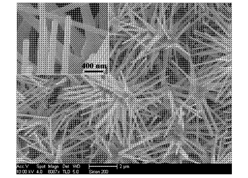
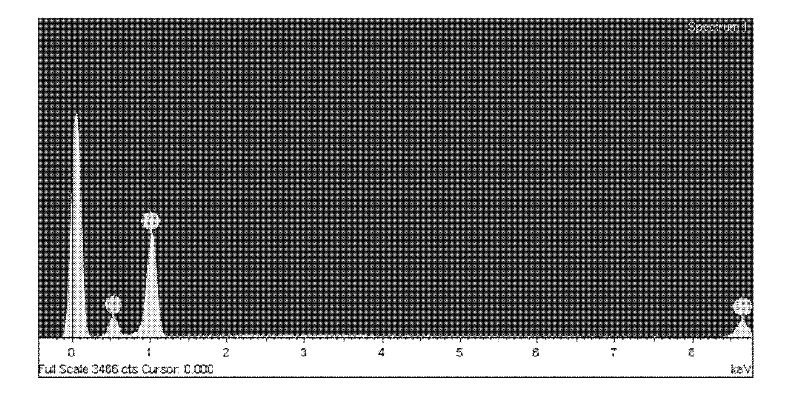
[0040] Step 1, after mixing and grinding zinc oxide powder and graphite powder at a mass ratio of 3:1, take 0.40g of the mixture and put it into a ceramic boat and place it in the center of the tube furnace; place the silicon wafer upright on the downstream side of the tube furnace At 10 cm in the center, the rough surface faces the direction of the mixed powder of zinc oxide and graphite, which serves as the substrate for the growth of zinc oxide nanostructures; the tube furnace is heated to 950 °C, the heating rate is 100 °C / min, and the holding time is 60 min. A zinc oxide flower-like structure similar to that shown in Figure (2) SEM results and corresponding to the EDS curve in Figure (3) was obtained, and a large number of zinc oxide nanorods grew on each flower-like unit.

[0041] In step 2, a gold film of about 3 nm is sputtered on the silicon wafer on which zinc oxide nanorods are grown, and then kept in air at 800° C. for 30 minutes to obtain an intermediate product. ...

Embodiment 2

[0043] The concrete steps of preparation are:

[0044] Step 1, after mixing and grinding zinc oxide powder and graphite powder at a mass ratio of 3.5:1, take 0.45g of the mixture and put it into a ceramic boat and place it in the center of the tube furnace; place the silicon chip upright in the downstream distance of the tube furnace At 10.5 cm in the center, the rough surface faces the direction of the mixed powder of zinc oxide and graphite, which is used as the substrate for the growth of zinc oxide nanostructures; the tube furnace is heated to 975 ° C, the heating rate is 100 ° C / min, and the holding time is 70 min. A zinc oxide flower-like structure similar to that shown in Figure (2) SEM results and corresponding to the EDS curve in Figure (3) was obtained, and a large number of zinc oxide nanorods grew on each flower-like unit.

[0045] In step 2, a gold film of about 2nm is sputtered on the silicon wafer grown with zinc oxide nanorods, and then kept in air at 850° C....

Embodiment 3

[0047] The concrete steps of preparation are:

[0048] Step 1, after mixing and grinding zinc oxide powder and graphite powder at a mass ratio of 4:1, take 0.50 g of the mixture and put it into a ceramic boat and place it in the center of the tube furnace; place the silicon wafer upright in the downstream distance of the tube furnace At 11cm in the center, the rough surface faces the direction of the mixed powder of zinc oxide and graphite, which is used as the substrate for the growth of zinc oxide nanostructures; the tube furnace is heated to 1000°C, the heating rate is 100°C / min, and the holding time is 80min. The ZnO flower-like structure shown in Figure (2) SEM results and corresponding to the EDS curve in Figure (3) was obtained, and a large number of ZnO nanorods grew on each flower-like unit.

[0049] In step 2, a gold film with a thickness of about 3 nm is sputtered on the silicon wafer grown with zinc oxide nanorods, and then kept in air at 900° C. for 50 minutes to ...


PUM

PropertyMeasurementUnit
diameteraaaaaaaaaa
diameteraaaaaaaaaa

Abstract

The invention relates to the field of nano material preparation, and specifically relates to a one-dimensional axial type nano zinc oxide / zinc sulfide heterojunction and a preparation method thereof. The prepared one-dimensional axial type comprises a zinc oxide nanorod and a zinc sulfide nanorod, and ends of the zinc oxide nanorod is connected with the zinc sulfide nanorod to form a heterojunction. A silicon chip, zinc oxide powder and graphite powder are mixed and placed in 950-1050 DEG C air for a insulation reaction; nano zinc oxide flower structures consisting a large amount of zinc oxide nanorods are obtained on the silicon chip; a layer of gold membrane with a certain thickness is sputtered on the silicon chip containing zinc oxide nanorods; finally, the silicon chip and the zinc sulfide powder are placed in high purity argon atmosphere for insulating reaction to obtain a final product the heterojunction with upper end of zinc oxide nanorod connected with zinc sulfide nanorod. The one-dimensional axial type heterojunction is easily prepared and at low costs. The heterojunction has great significance in development and application of nano device.

Description

technical field [0001] The invention belongs to the field of nanometer materials, and relates to a novel heterojunction and a preparation method thereof, in particular to a preparation method of a one-dimensional axial nanometer zinc oxide / zinc sulfide (ZnO / ZnS) heterojunction. Background technique [0002] A junction composed of two semiconductor single crystal materials with different bandgap widths is called a heterojunction. Due to the different physical parameters such as electron affinity and bandgap width of the two materials, the heterojunction has better properties than the p-n junction composed of the same material, such as higher electron injection ratio and window effect. [0003] One-dimensional nanomaterials refer to material systems in which carriers can move freely in only one direction and are constrained in the other two directions. One-dimensional zinc oxide (ZnO), as an important wide bandgap (3.37eV) semiconductor, has shown excellent performance in pho...

Claims


Application Information

Patent Timeline
Patent Type & Authority Applications(China)
IPC IPC(8): C30B25/18C30B23/02
Inventor 朱燕琴费广涛
Owner HEFEI INSTITUTES OF PHYSICAL SCIENCE - CHINESE ACAD OF SCI
Learn More