LED (Light-emitting Diode) device and wafer-level LED device as well as packaging structure of LED device and wafer-level LED device

A technology of LED devices and packaging structures, applied in the direction of electric solid-state devices, semiconductor devices, electrical components, etc., to achieve the effects of improving reliability, preventing absorption and scattering, and improving production efficiency

Inactive Publication Date: 2012-02-08
APT ELECTRONICS
View PDF5 Cites 15 Cited by
  • Summary
  • Abstract
  • Description
  • Claims
  • Application Information

AI Technical Summary

Problems solved by technology

Therefore, this requires that the ACF should preferably be a transparent material with a transmittance of 100%, otherwise it will have a great absorption effect on light, and at the same time, the conductive particles in the ACF will also have a great impact on the reflected light, further reducing the light of the LED. Extraction efficiency, thus, affects the light efficiency of LED devices

Method used


Image

  • LED (Light-emitting Diode) device and wafer-level LED device as well as packaging structure of LED device and wafer-level LED device
  • LED (Light-emitting Diode) device and wafer-level LED device as well as packaging structure of LED device and wafer-level LED device
  • LED (Light-emitting Diode) device and wafer-level LED device as well as packaging structure of LED device and wafer-level LED device

Examples


Embodiment 1

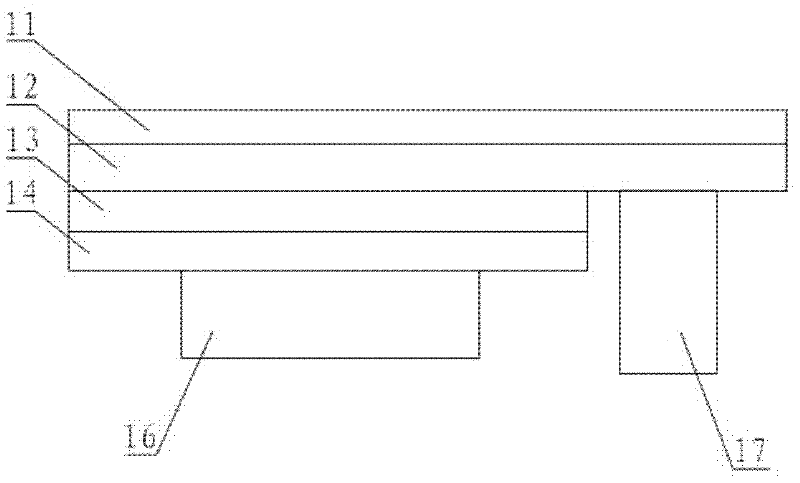
[0037] Such as figure 1 As shown, it is a schematic structural diagram of an existing LED chip, which includes a conventional sapphire substrate 11, N-type gallium nitride 12, light emitting layer 13, P-type gallium nitride 14, P electrode bumps 16 and N electrode bumps 17 , before flip-chip, the LED chip is located on the side of the P-type gallium nitride, which is the upper surface in the usual sense.

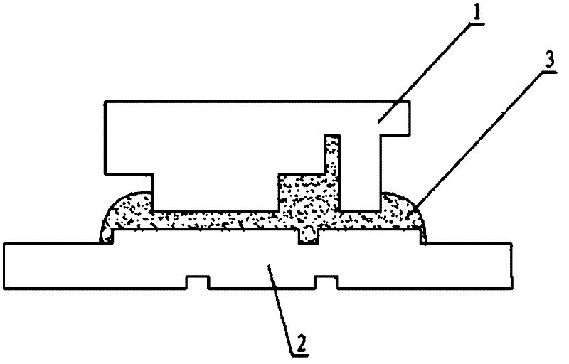
[0038] Such as figure 2 As shown, this embodiment discloses an LED device, including an LED chip 1 and a substrate 2, the LED chip 1 is flip-chip mounted on the substrate 2, and the electrical connection between the LED chip 1 and the substrate 2 is realized through the ACF 3, so that the two The electrical connection between them is more reliable. Wherein, the ACF includes bonding materials and conductive particles, the bonding materials include thermosetting materials and thermoplastic materials; the conductive particles include any of the following metal flexor materi...

Embodiment 2

[0050] Such as Figure 7 As shown, the difference between this embodiment and embodiment 1 is:

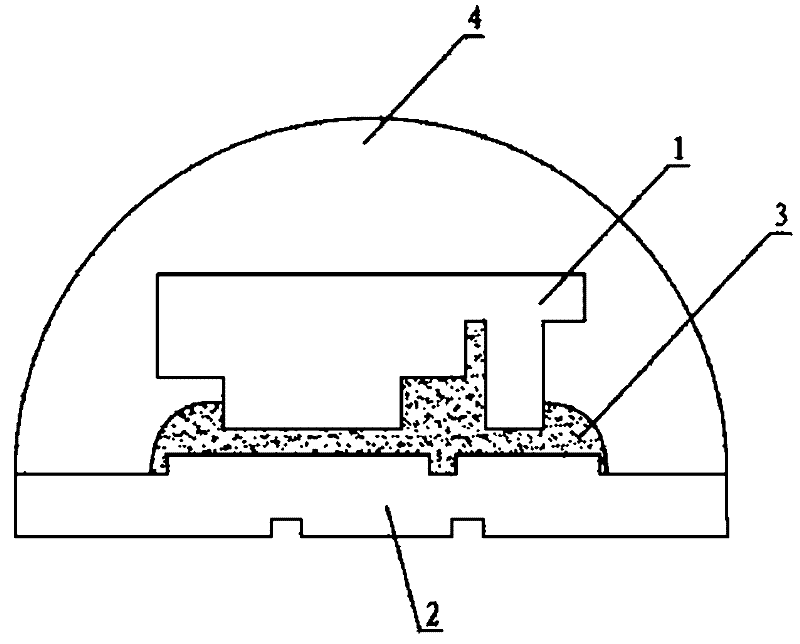
[0051] In this embodiment, gold flex wires 26 are used to connect the first gold flex electrode layer 22 and the second gold flex electrode layer 24 from the side to the bottom of the substrate 2, and the optical structure layer 42 in the outer packaging layer 4 has a square shape. The optical structure layer 42 is used for the adjustment of the external shape, which can realize the different optical type requirements of the packaging structure, and its material can be polycarbonate (PC), polymethyl methacrylate (PMMA), silica gel (Silicone), poly One or more of propylene (EP), polyethylene phthalate (PET), and glass. The square shape structure can be made into a small volume and easy to form.

Embodiment 3

[0053] This embodiment also discloses an LED device. The difference between this embodiment and Embodiment 1 is that the specific position of the reflective layer is slightly changed, such as Figure 8 Shown:

[0054] Its LED chip 1 includes a conventional sapphire substrate 11, N-type gallium nitride 12, light-emitting layer 13, P-type gallium nitride 14, P-electrode bumps 16 and N-electrode bumps 17; An ohmic contact layer 18 is grown on the P-type gallium nitride 14, and the conductive or non-conductive reflective layer 15 covers the outer surface of the ohmic contact layer on both sides of the P electrode bump of the LED chip. The P electrode bump 16 is directly electrically connected with the P-type gallium nitride 14 through the ohmic contact layer 18. At this time, the reflective layer 15 can be a distributed Bragg reflective layer (non-conductive reflective layer) composed of aluminum oxide, silicon dioxide, and titanium dioxide. ), or the reflective layer 15 is a gol...


PUM


Abstract

The invention belongs to the technical field of LED and particularly discloses an LED (Light-emitting Diode) device and a wafer-level LED device as well as a packaging structure of the LED device and the wafer-level LED device. In the invention, a reflecting layer is placed on the upper surface of an LED chip and the LED chip is reversely arranged on a substrate through an ACF (Active Carbon Fiber), so that the packaging reliability is improved, the absorption and the radiation of the ACF to lights are effectively prevented and the lighting effect is further improved; and meanwhile, the ACF is not limited by the selection of the materials, the wafer-level encapsulating is easy to realize and the production efficiency is improved.

Description

technical field [0001] The invention belongs to the technical field of LEDs, and in particular relates to a flip-chip LED device, a wafer-level LED device and their packaging structures. Background technique [0002] Light-emitting diode (LED) is an electroluminescent device processed by semiconductor manufacturing technology. The main principle of light emission is that the compound semiconductor material is loaded with a forward voltage, and active electrons and holes recombine to generate photons, of which the wavelength of 380-780 nanometers The light that can be recognized by the human eye is called visible light. At present, because the light efficiency of LEDs has been greatly improved, LEDs are widely used in various fields, including backlight units, automobiles, electric signals, traffic lights, lighting devices, and the like. [0003] According to different packaging structures, LEDs can be divided into three types: front-mount, flip-chip, and vertical. [0004...

Claims


Application Information

Patent Timeline
Patent Type & Authority Applications(China)
IPC IPC(8): H01L33/62H01L25/075
CPCH01L24/32H01L2924/01322H01L2924/12041H01L2924/15787H01L2924/15788
Inventor 纪玲玲区伟能万垂铭何贵平陈海英
Owner APT ELECTRONICS
Why Eureka
Try Eureka