
High-voltage nitride-based LED (light emitting diode) device and manufacturing method thereof

A technology for LED devices and manufacturing methods, which is applied to semiconductor devices, electro-solid devices, electrical components, etc., can solve the problems of low yield and high cost of LED chips and lamps, so as to achieve customization, improve yield and packaging. Efficiency, lead count and package space savings

Inactive Publication Date: 2012-02-15
ENRAYTEK OPTOELECTRONICS
View PDF8 Cites 21 Cited by
  • Summary
  • Abstract
  • Description
  • Claims
  • Application Information

AI Technical Summary

Problems solved by technology

However, there are still considerable barriers in the actual implementation process, and it is urgent to introduce new methods that can effectively improve the above defects, so as to solve the high cost of LED chip industry, high lamp price and low yield rate when using third-generation semiconductor materials. The problem

Method used


Image

  • High-voltage nitride-based LED (light emitting diode) device and manufacturing method thereof
  • High-voltage nitride-based LED (light emitting diode) device and manufacturing method thereof
  • High-voltage nitride-based LED (light emitting diode) device and manufacturing method thereof

Examples


Embodiment Construction

[0015] In order to make the above objects, features and advantages of the present invention more comprehensible, specific implementations of the present invention will be described in detail below in conjunction with the accompanying drawings.

[0016] In the following description, numerous specific details are set forth in order to provide a thorough understanding of the present invention. However, the present invention can be implemented in many other ways different from those described here, and those skilled in the art can make similar extensions without violating the connotation of the present invention, so the present invention is not limited by the specific implementations disclosed below.

[0017] Secondly, the present invention is described in detail using schematic diagrams. When describing the embodiments of the present invention in detail, for the convenience of explanation, the cross-sectional view showing the device structure will not be partially enlarged accordi...


PUM


Abstract

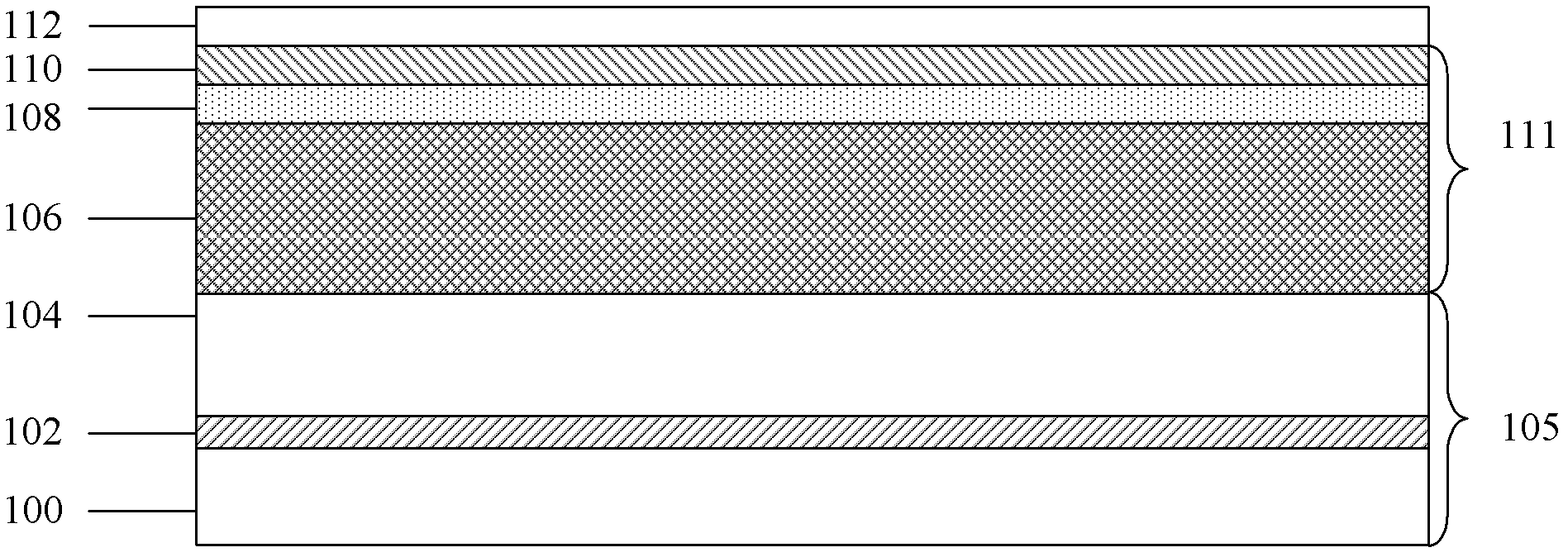
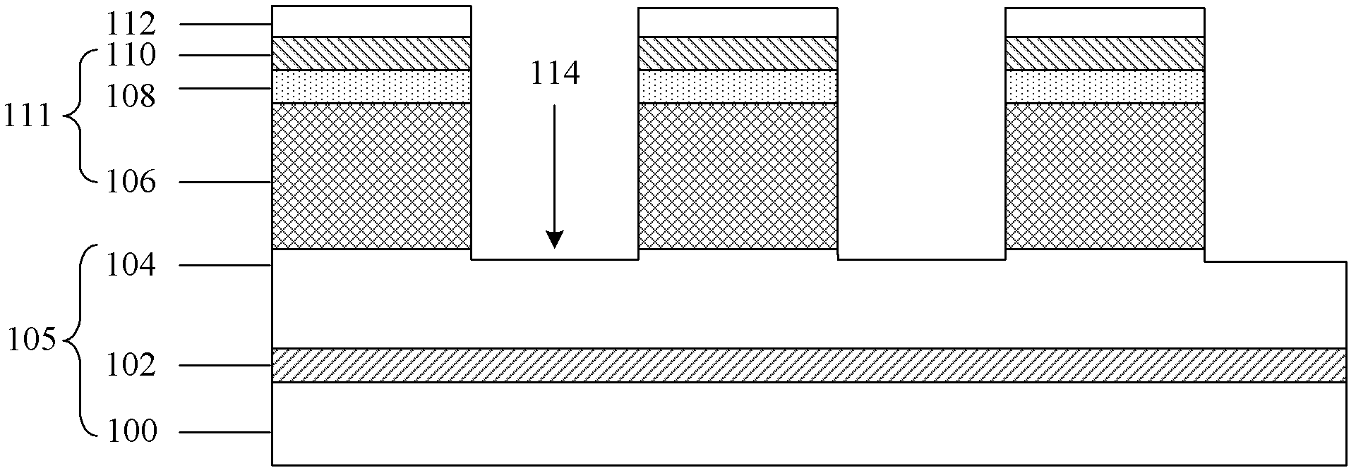
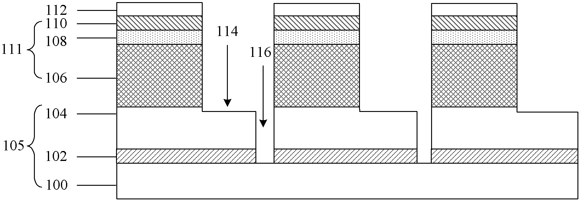
The invention provides a manufacturing method of a high-voltage nitride-based LED (light emitting diode) device, which comprises the following steps of: providing a substrate, and sequentially forming N-type nitride nucleating layers and epitaxial layers on the substrate; etching the epitaxial layers to form N-type contact electrode steps; sequentially etching the N-type nitride nucleating layers to form LED isolation trenches which are exposed out of the surface of the substrate; manufacturing N-type contact electrodes on the N-type contact electrode steps and manufacturing P-type contact electrodes on the epitaxial layers to form a plurality of LED unit chips; and carrying out photoelectric performance test on the LED unit chips, and carrying out laser scribing on the LED unit chips selectively according to a test result so as to cut the LED unit chips in groups to form at least one LED module. The invention also provides the high-voltage nitride-based LED device, so that the cost of the whole LED chip industry is reduced, and the yield is improved.

Description

technical field [0001] The invention belongs to the field of light-emitting device manufacturing, and in particular relates to a high-voltage nitride LED device and a manufacturing method thereof. Background technique [0002] With the development of nitride-based high-brightness light-emitting diode (Light Emitting Diode, LED) application development, a new generation of green and environmentally friendly solid-state lighting source nitride LED has become the focus of research, especially the third-generation semiconductor gallium nitride ( GaN) represented by the development of blue LED. Group III nitride semiconductor materials based on gallium nitride (GaN), indium gallium nitride (InGaN) and aluminum gallium nitride (AlGaN) alloys have wide direct band gaps, high internal and external quantum efficiencies, high thermal conductivity, and High temperature, corrosion resistance, shock resistance, high strength and high hardness are ideal materials for manufacturing high-b...

Claims


Application Information

Patent Timeline
Patent Type & Authority Applications(China)
IPC IPC(8): H01L27/15H01L33/02H01L33/36H01L33/00H01L33/48H01L33/62
CPCH01L2224/48091H01L2224/48137H01L2224/48464H01L2224/49107H01L2224/73265H01L2924/00014
Inventor 肖德元于洪波于婷婷程蒙召张汝京
Owner ENRAYTEK OPTOELECTRONICS
Learn More