Semiconductor device used for SOI (silicon-on-insulator) high-voltage integrated circuit

A high-voltage integrated circuit and semiconductor technology, applied in semiconductor devices, electric solid devices, circuits, etc., can solve the problems of difficult to withstand voltage exceeding 600V, large parasitic effect, deep groove etching, etc., and achieve the improvement and reduction of breakdown voltage Thickness, process to achieve simple effect

Inactive Publication Date: 2012-02-22
UNIV OF ELECTRONICS SCI & TECH OF CHINA
View PDF12 Cites 17 Cited by
  • Summary
  • Abstract
  • Description
  • Claims
  • Application Information

AI Technical Summary

Problems solved by technology

[0007] The technical problem to be solved by the present invention is that the top layer silicon and the dielectric buried layer of the existing SOI high-voltage integrated circuit semiconductor device are relatively thick, which has serious self-heating effect, large parasitic effect, deep groove etching and filling, and high withstand voltage. It is difficult to exceed 600V, etc., and provide a set of SOI high-voltage integrated circuit semiconductor devices (including high-voltage NMOS, high-voltage PMOS, high-voltage LIGBT, low-voltage NMOS, and low-voltage PMOS) with relatively thin top silicon and dielectric buried layers, which have low leakage and occupy chips. The characteristics of small area, high speed, high integration, low power consumption, and simple process can meet the needs of 1200V SOI high-voltage integrated circuits

Method used


Image

  • Semiconductor device used for SOI (silicon-on-insulator) high-voltage integrated circuit
  • Semiconductor device used for SOI (silicon-on-insulator) high-voltage integrated circuit
  • Semiconductor device used for SOI (silicon-on-insulator) high-voltage integrated circuit

Examples


Embodiment Construction

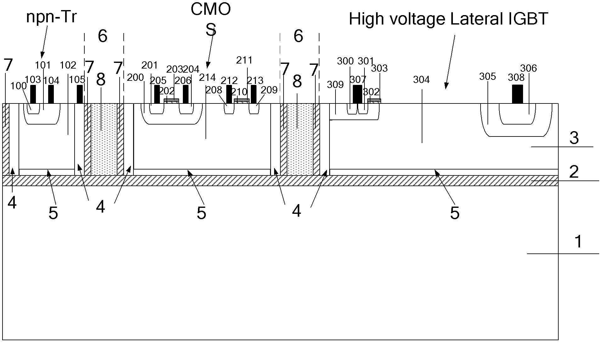
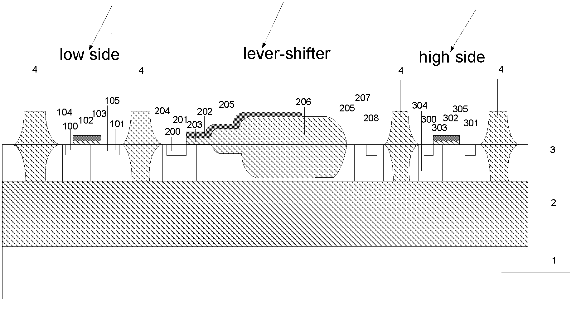
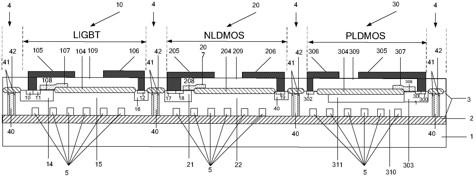
[0038] In order to make the technical problems, technical solutions and beneficial effects to be solved by the present invention clearer, the present invention will be further described in detail below in conjunction with the accompanying drawings and embodiments. It should be understood that the specific examples given here are only used to explain the present invention, not to limit the present invention. Example of structure diagram of semiconductor device used in SOI high voltage integrated circuit according to the present invention Figure 4 shown, where the high-voltage NLDMOS device results as Figure 5-8 , the high-voltage PLDMOS device results as Figures 9 to 12 , the high-voltage NLIGBT device results as Figures 13 to 16 .

[0039] image 3 It is a structural schematic diagram of the SOI high-voltage integrated circuit semiconductor device of the present invention. It includes a semiconductor substrate layer 1, a dielectric buried layer 2, and a top layer of s...


PUM


Abstract

The invention relates to a semiconductor device used for an SOI (silicon-on-insulator) high-voltage integrated circuit, belonging to the field of power semiconductor devices. The semiconductor device comprises a semiconductor substrate layer, a dielectric buried layer and a silicon top layer, wherein at least high-voltage LIGBT (lateral insulated gate bipolar transistor), NLDMOS (N-type lateral double-diffused metal-oxide semiconductor) and PLDMOS (P-type lateral double-diffused metal-oxide semiconductor) devices are integrated in the silicon top layer; the thickness of the dielectric buried layer is not more than 5 mum; the thickness of the silicon top layer is not more than 20 mum; multiple incontinuous high-concentration N<+> regions (doping concentration is not lower than 1e16e cm<-3>) are formed at the bottoms of the high-voltage devices and the silicon top layer above the surface of the dielectric buried layer; the high-voltage devices are isolated by dielectric isolation regions; low-voltage MOS (metal oxide semiconductor) devices can also be integrated in the device; the high-voltage devices and low-voltage devices are isolated by the dielectric isolation regions; and different low-voltage devices are isolated by field oxidation layers. The semiconductor device has the advantages that: because of the introduction of the multiple incontinuous high-concentration N<+> regions, the electric field of the silicon top layer is weakened and the electric field of the dielectric buried layer is enhanced at the same time, the breakdown voltage of the device is greatly improved, and the device can be applied in high-voltage integrated circuits in the automobile electronics, consumption electronics, green lighting, industrial control, power supply management, display driving and other fields.

Description

technical field [0001] The invention belongs to the technical field of power semiconductor devices, and more specifically relates to a semiconductor device used for SOI (Silicon On Insulator) high-voltage integrated circuits. Background technique [0002] SOI high voltage integrated circuit (High Voltage Integrated Circuit, HVIC) is widely used in automotive electronics, consumer electronics, green lighting, industrial control, power management, display drive due to its advantages of high speed, low power consumption, radiation resistance and easy isolation However, since the longitudinal withstand voltage of SOI high-voltage devices is limited by the thickness of the dielectric layer, the application range of commercial SOI high-voltage integrated circuits has only reached the high-voltage field of 600V. For the high-voltage field above 600V, such as 1000V and 1200V, there is no commercial SOI high-voltage integrated circuit product yet. [0003] Document 1 N.Yasuhara, A.N...

Claims


Application Information

Patent Timeline
Patent Type & Authority Applications(China)
IPC IPC(8): H01L27/12H01L29/06H01L29/36
Inventor 乔明周锌温恒娟何逸涛章文通向凡叶俊张波
Owner UNIV OF ELECTRONICS SCI & TECH OF CHINA
Why Eureka
Try Eureka