Integrated light-emitting diode array chip and production method thereof

An integrated technology of light-emitting diodes, applied in semiconductor/solid-state device manufacturing, electrical components, electric solid-state devices, etc., can solve the problems of power loss, chip loss, uneven brightness, etc., achieve less heat generation, save packaging costs, current good extension effect

Inactive Publication Date: 2012-03-14
DALIAN MEIMING EPITAXIAL WAFER TECH
View PDF4 Cites 17 Cited by
  • Summary
  • Abstract
  • Description
  • Claims
  • Application Information

AI Technical Summary

Problems solved by technology

Moreover, the chips used in the above traditional methods are all independent, and there are still problems suc...

Method used


Image

  • Integrated light-emitting diode array chip and production method thereof
  • Integrated light-emitting diode array chip and production method thereof
  • Integrated light-emitting diode array chip and production method thereof

Examples


Embodiment 1

[0037] The manufacturing method of the integrated light emitting diode array chip comprises the following steps:

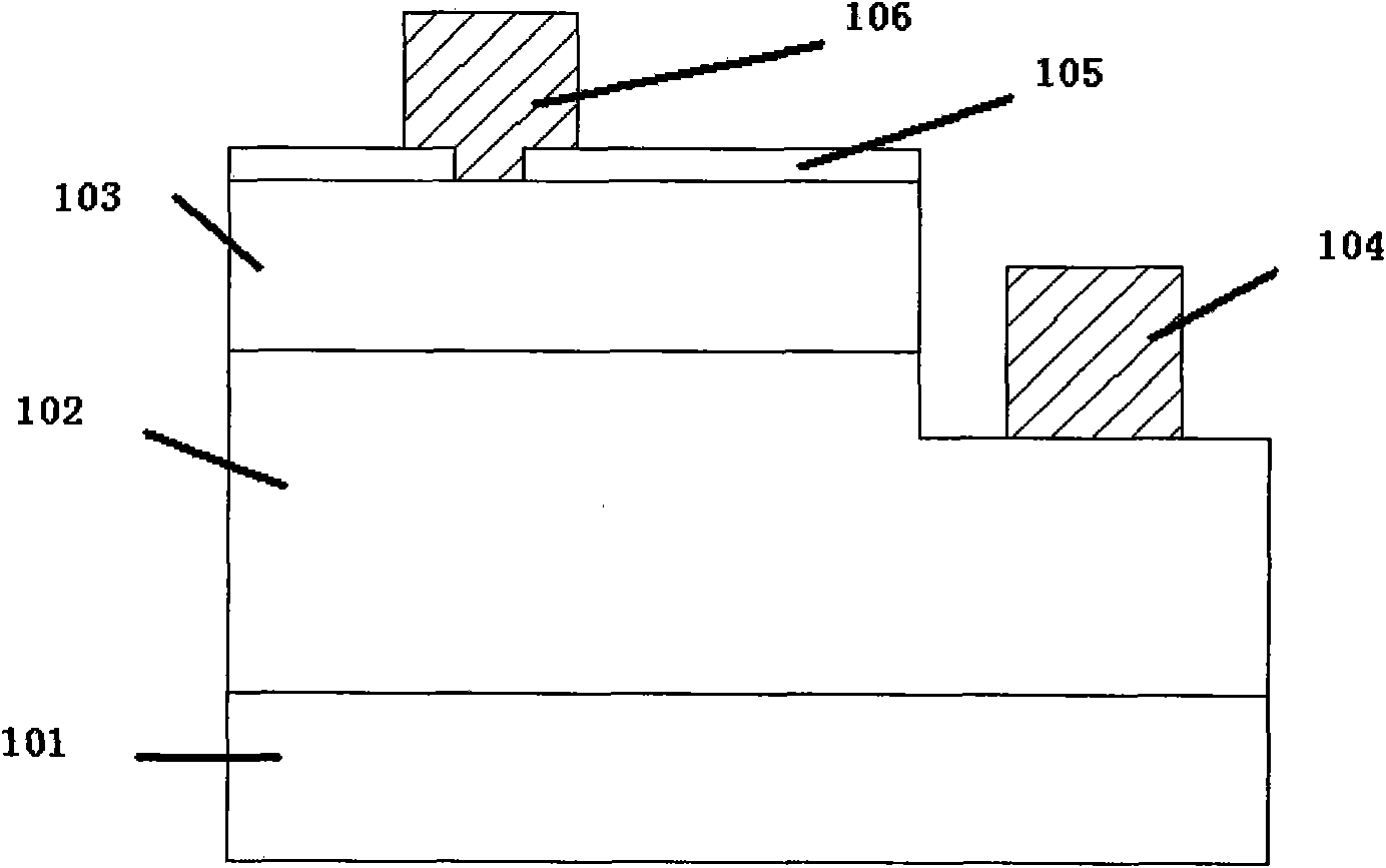
[0038] 1. Evaporate the ITO current spreading layer 105 on the P-type GaN epitaxial layer of the GaN epitaxial wafer by electron beam evaporation, the evaporation environment temperature is 230-250°C, and the thickness is between Then anneal in a suitable environment, the temperature is 250-700 ° C, and the time is 10-60 minutes to form a transparent P-type ohmic contact layer, and then follow the reference figure 2 The designed pattern uses photoresist as a mask, retains the part of the pre-designed transparent electrode layer, uses the method of chemical wet etching, uses ITO etching solution: FeCl3+HCl, soaks at 40 ° C for 5 minutes, and removes the remaining part. ITO current spreading layer.

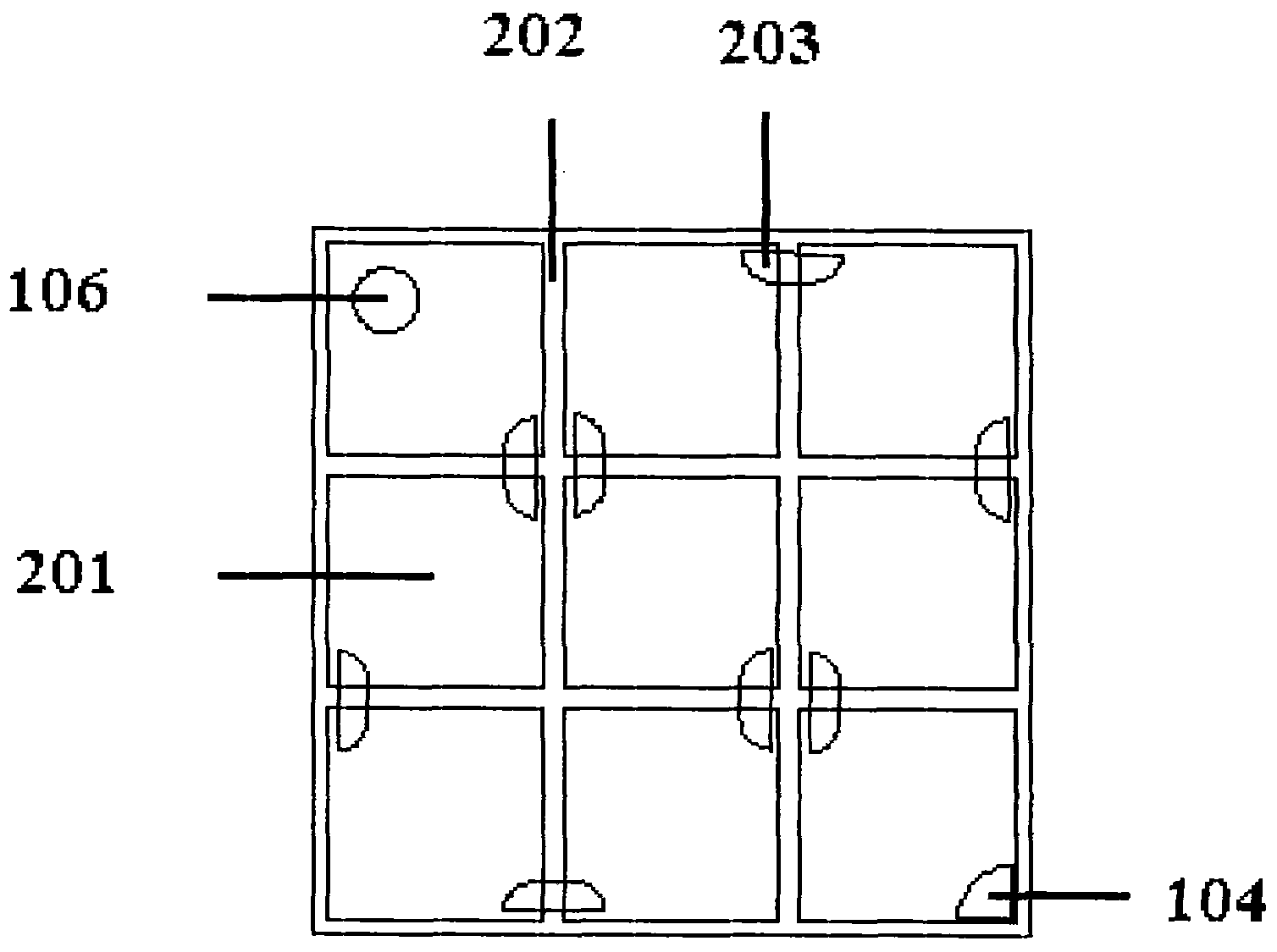
[0039] 2. Using ICP dry etching, the grown epitaxial wafer is etched according to the pre-designed pattern, and every two light-emitting structures are an integrated...

Embodiment 2

[0046] The manufacturing method of the integrated light emitting diode array chip comprises the following steps:

[0047] 1. Evaporate the ITO current spreading layer 105 on the P-type GaN epitaxial layer of the GaN epitaxial wafer by electron beam evaporation, the evaporation environment temperature is 230-250°C, and the thickness is between Then anneal in a suitable environment, the temperature is 250-700 ° C, and the time is 10-60 minutes to form a transparent P-type ohmic contact layer, and then follow the reference figure 2 The designed pattern uses photoresist as a mask, retains the part of the pre-designed transparent electrode layer, uses the method of chemical wet etching, uses ITO etching solution: FeCl3+HCl, soaks at 40 ° C for 5 minutes, and removes the remaining part. ITO current spreading layer.

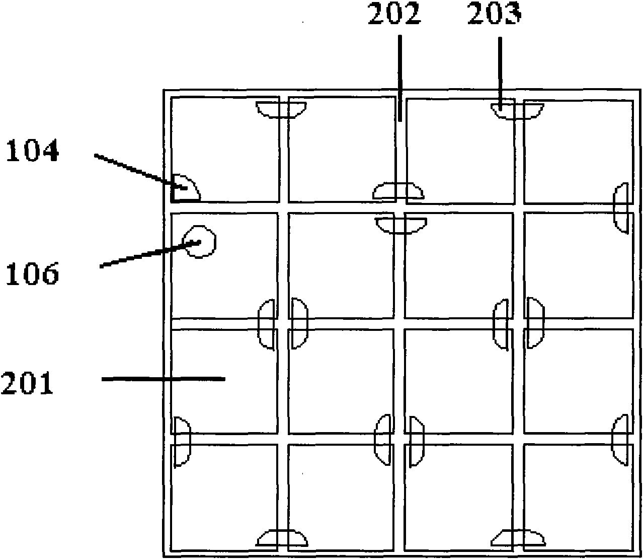
[0048] 2. Using ICP dry etching, the grown epitaxial wafer will be etched according to the pre-designed pattern, and every 25 light-emitting structures will be an in...

Embodiment 3

[0055] The manufacturing method of the integrated light emitting diode array chip comprises the following steps:

[0056] 1. Evaporate the ITO current spreading layer 105 on the P-type GaN epitaxial layer of the GaN epitaxial wafer by electron beam evaporation, the evaporation environment temperature is 230-250°C, and the thickness is between Then anneal in a suitable environment, the temperature is 250-700 ° C, and the time is 10-60 minutes to form a transparent P-type ohmic contact layer, and then follow the reference figure 2 The designed pattern uses photoresist as a mask, retains the part of the pre-designed transparent electrode layer, uses the method of chemical wet etching, uses ITO etching solution: FeCl3+HCl, soaks at 40 ° C for 5 minutes, and removes the remaining part. ITO current spreading layer.

[0057] 2. Using ICP dry etching, the grown epitaxial wafer is etched according to the pre-designed pattern, and every 9 light-emitting structures are an integrated u...


PUM


Abstract

The invention relates to a production method of an integrated light-emitting diode array chip based on a gallium-nitride-based light-emitting diode. The production method comprises the following steps of: arranging 9 or 12 light-emitting diode units in an array manner to form a 3*3 or 3*4 matrix, and integrating the matrix in a chip; in the integrated chip, etching an insulating sapphire substrate layer through an etching technology to completely separate gallium nitride layers among the units; filling gaps among the units by using an insulating material, and covering the whole chip; opening electrode ports of the units on an insulating layer; connecting the electrode ports of the units in a metal evaporation manner so that the units in the whole chip form a circuit in a serial connection manner; and making P and N routing disc ports at both ends of the chip for accessing other circuits when the capsulation is carried out. The integrated chip produced by the production method has the advantages of high light-emitting strength and high photoelectric conversion efficiency and is beneficial to the capsulation and the design of a drive circuit. The production method is mainly applied to an illumination field.

Description

technical field [0001] The invention relates to an integrated light-emitting diode array chip and a manufacturing method thereof, belonging to the field of semiconductor lighting. Background technique [0002] Light-emitting diode (LED) is a light-emitting device that converts electrical energy into light energy. It is widely used in indication, display, decoration, lighting and many other fields, and has become an indispensable part of our life. The light-emitting diodes used in the above applications are packaged by light-emitting diode chips to realize their application functions. The core of a light emitting diode device is a light emitting diode chip. During the packaging process, the light-emitting diode chip becomes an easy-to-use device through optical, mechanical, thermal and electrical design, and this device can be used more reasonably and effectively for application needs. The invention relates to a novel design and manufacturing method of a light-emitting diod...

Claims


Application Information

Patent Timeline
IPC IPC(8): H01L27/15H01L21/782
Inventor 肖志国张帆武胜利陈向东郑远志阎小红
Owner DALIAN MEIMING EPITAXIAL WAFER TECH
Why Eureka
Try Eureka