Uncooled infrared detector device and manufacturing method thereof

A technology of uncooled infrared and production methods, which is applied in the field of infrared detection, can solve problems such as large working voltage, achieve easy excitation, and improve the effect of voltage temperature response coefficient

Inactive Publication Date: 2012-03-14
INST OF MICROELECTRONICS CHINESE ACAD OF SCI
View PDF3 Cites 2 Cited by
  • Summary
  • Abstract
  • Description
  • Claims
  • Application Information

AI Technical Summary

Problems solved by technology

[0005] The voltage temperature response coefficient is an important parameter to determine the temperature sensitivity of the uncooled infrared detector. At present, in the single crystal silicon PN junction diode type infrared detector, the forward voltage temperature response coefficient of the diode is about 1.3mV / K. By changing a single Various process parameters of the diode have little effect on the temperature response coefficient of the forward voltage of the diode. Usually, multiple diodes (such as 6-8) need to be connected in series to improve the overall temperature sensitivity of the infrared detector and meet the needs of practical applications. However, multiple diodes connected in series will result in a larger operating voltage (usually higher than 6V) for single crystal silicon PN junction diode type infrared detectors.

Method used


Image

  • Uncooled infrared detector device and manufacturing method thereof
  • Uncooled infrared detector device and manufacturing method thereof
  • Uncooled infrared detector device and manufacturing method thereof

Examples


Embodiment 1

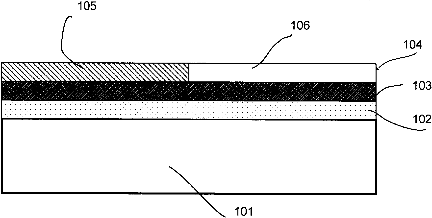
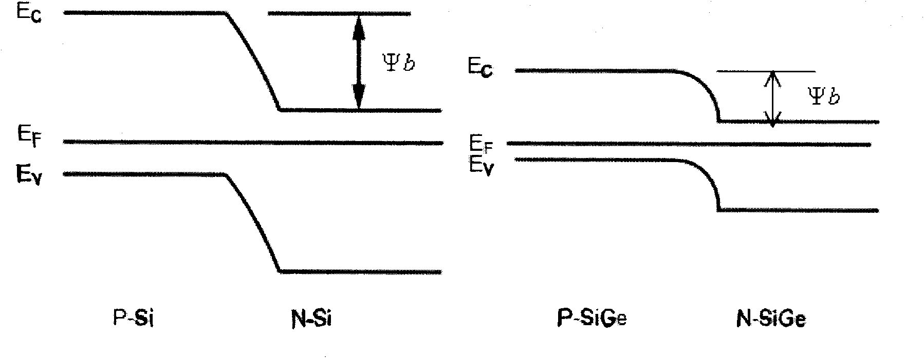
[0052] figure 1 It is a schematic structural diagram of the uncooled infrared detection device in this embodiment, figure 2 It is a diagram comparing the energy bands of the SiGe PN junction and the traditional single crystal silicon PN junction in this embodiment.

[0053] Such as figure 1 As shown, uncooled infrared detectors include:

[0054] SOI (Silicon On Insulator, silicon on insulator) substrate;

[0055] Si on the SOI substrate x Ge 1-x layer 104, and the SiGe layer 104 includes adjacent P-type regions 105 and N-type regions 106.

[0056] Wherein, the SOI substrate is composed of a bottom silicon layer 101, a buried oxide layer 102 and a top silicon layer 103, both of which are monocrystalline silicon materials. For an infrared detection device, the top silicon layer 103 and the buried oxide layer 102 should be as thin as possible, and the thickness range is, for example, 50nm-200nm. The SOI substrate is made by implanting oxygen ions on a single crystal silic...

Embodiment 2

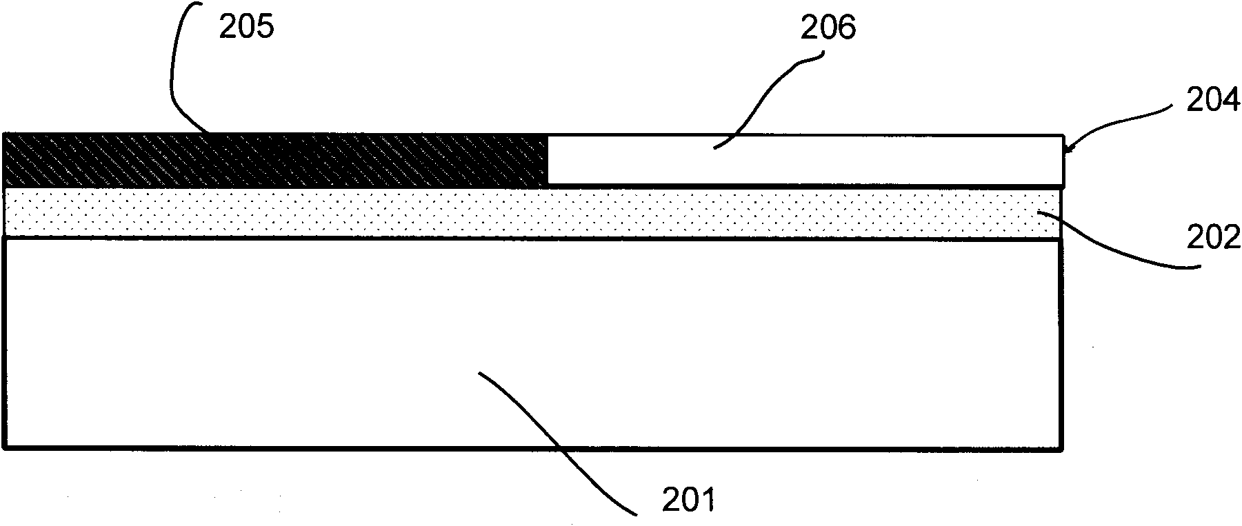
[0071] image 3 It is a schematic structural diagram of the uncooled infrared detection device in this embodiment. As shown in the figure, the uncooled infrared detector includes:

[0072] a single crystal silicon substrate 201, the single crystal silicon substrate 201 has a buried oxide layer 202;

[0073] Si on the buried oxide layer 202 x Ge 1-x layer 204, the Si x Ge 1-x Layer 204 includes adjacent P-type regions 205 and N-type regions 206 .

[0074] The difference from Example 1 is that the Si x Ge 1-x Layer 204 is on buried oxide layer 202 rather than on the top silicon layer.

[0075] The substrate of this embodiment does not have a top silicon layer, and the specific manufacturing method is: first epitaxially grow Si on the single crystal silicon substrate. x Ge 1-x layer, followed by oxygen ion implantation on the monocrystalline Si substrate and Si x Ge 1-x A buried oxide layer is formed at the interface of the layer, and then Si is formed by photolithogra...

Embodiment 3

[0079] Figure 4 It is a schematic structural diagram of the uncooled infrared detection device in this embodiment, Figure 5 Si in this example x Ge 1-x Energy band comparison diagram of / Si heterojunction and traditional single crystal silicon PN junction.

[0080] Such as Figure 4 As shown, the uncooled infrared detection device includes:

[0081] SOI substrate, the SOI substrate has an N-type top silicon layer 303;

[0082] The P-type Si on the N-type top silicon layer 303 x Ge 1-x layer 305, the P-type Si x Ge 1-x Layer 305 is grown using selective epitaxy.

[0083] Wherein, the SOI substrate is composed of a bottom silicon layer 301 , a buried oxide layer 302 and a top silicon layer 303 , and both the bottom silicon layer 301 and the top silicon layer 303 are made of single crystal silicon. N-type top silicon layer 303 and P-type Si x Ge 1-x Layer 305 constitutes a SiGe / Si heterojunction diode.

[0084] The manufacturing method of the above-mentioned uncool...


PUM


Abstract

The invention provides an uncooled infrared detector device and a manufacturing method thereof. The uncooled infrared detector device comprises a substrate and a SiGe layer arranged on the substrate, wherein the substrate comprises an insulating layer, and the SiGe layer comprises a P-type area and an N-type area which are adjacent to each other. Correspondingly, the invention further provides another uncooled infrared detector device which comprises an SOI (Silicon on Insulator) substrate and a P-type SiGe layer, wherein the SOI substrate has an N-type top silicon layer; the P-type SiGe layer is arranged on the N-type top silicon layer; and the P-type SiGe layer is selectively epitaxial grown. In the uncooled infrared detector device, the P-type area of a diode is made of a SiGe material, thereby forming a SiGe PN junction diode or SiGe / Si heterojunction diode so as to reduce a working voltage. A forbidden bandwidth of the SiGe material changes within a range of 0.66-1.12eV following the change of Ge components. Relative to a monocrystalline silicon diode, the forbidden bandwidth of the SiGe material is narrower, thereby being easier to stimulate the forming of the PN junction diode and promoting a voltage temperature response coefficient.

Description

technical field [0001] The invention relates to the technical field of infrared detection, in particular to an uncooled infrared detection device and a manufacturing method thereof. Background technique [0002] Infrared detection devices are the core components of thermal imaging systems, and are mainly divided into two categories: cooling type (based on photon detection) and uncooled type (based on thermal detection), the former was once considered to be the best infrared thermal detection technology in practical applications, However, due to the need to match the refrigeration device, its manufacturing and use costs are relatively high. [0003] In recent years, uncooled infrared detection devices have made great progress. Compared with cooled infrared detection devices, uncooled infrared detection devices do not need to install cooling devices in thermal imaging systems, so they are smaller in size, lighter in weight and lower in power consumption; In addition, wider sp...

Claims


Application Information

Patent Timeline
Patent Type & Authority Applications(China)
IPC IPC(8): H01L31/101H01L31/028H01L31/18
CPCY02P70/50
Inventor 欧文何伟陈大鹏
Owner INST OF MICROELECTRONICS CHINESE ACAD OF SCI
Why Eureka
Try Eureka