Solar-grade silicon wafer being cut by diamond wire and cutting method thereof

A diamond wire and cutting method technology, applied in stone processing equipment, fine working devices, manufacturing tools, etc., can solve the problems of low cutting efficiency, large environmental impact, waste of silicon powder, etc., achieve fast cutting speed, change high pollution , the effect of saving silicon resources

Inactive Publication Date: 2012-03-28
江西金葵能源科技有限公司
View PDF7 Cites 27 Cited by
  • Summary
  • Abstract
  • Description
  • Claims
  • Application Information

AI Technical Summary

Problems solved by technology

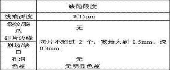
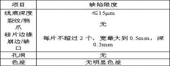
The traditional cutting process adopts the method of adding silicon carbide into the cutting fluid to form a free mortar for wire cutting. During the cutting process, since silicon carbide is in a free state in the cutting fluid, it is also moving when it moves with the cutting wire. There will be indole-like cut marks on the surface of the cut silicon wafer, which will cause a large number of loss layers on the surface of the silicon wafer, which will reduce the photoelectric conversion efficiency of the single crystal silicon wafer. At the same time, it also has the following problems:
[0004] 1. Using free mortar for cutting, the cutting cost is high; after cutting, the mortar is difficult to recycle and has a great impact on the environment;
[0005] 2. During the cutting process, 40% of silicon powder will be wasted, and silicon powder cannot be recycled by using traditional techniques;
[0006] 3. The cutting efficiency is low, a single cutting takes 7-8 hours, and the cutting efficiency is relatively low

Method used


Image

  • Solar-grade silicon wafer being cut by diamond wire and cutting method thereof
  • Solar-grade silicon wafer being cut by diamond wire and cutting method thereof
  • Solar-grade silicon wafer being cut by diamond wire and cutting method thereof

Examples


Embodiment Construction

[0036] In order to understand the present invention more clearly, describe the present invention in detail in conjunction with embodiment:

[0037] The diameter of the diamond steel wire used is 150um, the slot distance of the slot wheel used is 345um, the diamond wire cutting machine model is Takatori MWS4450D; the raw material is 125×125mm solar single crystal square rod, the following is the use of diamond wire cutting machine to cut single crystal silicon wafers Production method and specific process:

[0038] (1) Adhesive rods: Before bonding the single crystal silicon rods, the surface of the single crystal silicon rods is treated, and the bonding surface of the single crystal silicon rods is wiped with absolute ethanol. The adhesive uses American AB glue, and the connecting material uses resin strips , during the curing process of the glue, use 5-10kg pressure weight to pressurize the monocrystalline silicon rod to discharge excess glue; the pressurization time is 0...


PUM


Abstract

The invention discloses a solar-grade silicon wafer being cut by a diamond wire and a cutting method thereof. A mono-crystalline silicon square rod is cut by a diamond wire. The cutting method comprises the following steps that: the mono-crystalline silicon square rod which is formed by squaring, grinding and sharpening a mono-crystalline silicon circular rod, the mono-crystalline silicon square rod is fixed on a resin strip through an adhesive bar, the resin strip is fixed on an adhesive plate, then the adhesive plate and the mono-crystalline silicon square rod are collectively placed into a working cabin to be preheated, cutting liquid is circulated in the working cabin to work, then the diamond cutting is performed, the cut mono-crystalline silicon wafer is inversely arranged on a degumming device to degum, and the mono-crystalline silicon wafer is washed by ultrasonic and then is centrifugally dehydrated. Due to the adoption of the cutting method, the photoelectric conversion efficiency and the cutting efficiency of the mono-crystalline silicon wafer can be improved, a silicon wafer with the thickness of 140 to 200 micrometers can be produced, the qualification rate of the product can reach more than 98 percent; and silicon powder is recyclable, so valuable silicon resource can be saved, and the environment-friendly production can be really realized during the production process.

Description

technical field [0001] The invention relates to a solar grade single silicon wafer cut by diamond wire and a cutting process method thereof. Background technique [0002] Solar monocrystalline silicon wafers are used in solar cells, and monocrystalline silicon rods are processed into silicon wafers by wire cutting machines. At present, the multi-wire cutting machines of NTC, MB and HTC are generally used in the market for cutting processing. The cutting conditions are: the diameter of the wire cutting steel wire is 150um, and the groove distance on the main roller is 340um. The thickness of the silicon wafer is within the range of 200±20mm, the wire consumption of a single wafer is 1.06m, and the waste of silicon powder is 40%. [0003] At present, high cost is still the main obstacle restricting the large-scale application of photovoltaic power generation. In the production of silicon wafers, enterprises are required to improve production efficiency, reduce processing loss...

Claims


Application Information

Patent Timeline
Patent Type & Authority Applications(China)
IPC IPC(8): B28D5/04
Inventor 于景俞建业曾斌叶平欧阳思周汤玮胡凯
Owner 江西金葵能源科技有限公司
Why Eureka
Try Eureka