

Organic electroluminescent element
An electroluminescent element and luminescent technology, applied in the direction of electroluminescent light source, electrical components, electric light source, etc., can solve the problems of quenching luminescence, complicated process, and increase of product manufacturing cost, and achieve simple and simplified forming process Manufacturing process, the effect of reducing the number
- Summary
- Abstract
- Description
- Claims
- Application Information
AI Technical Summary
Problems solved by technology
Method used
Image

Examples
Embodiment 1
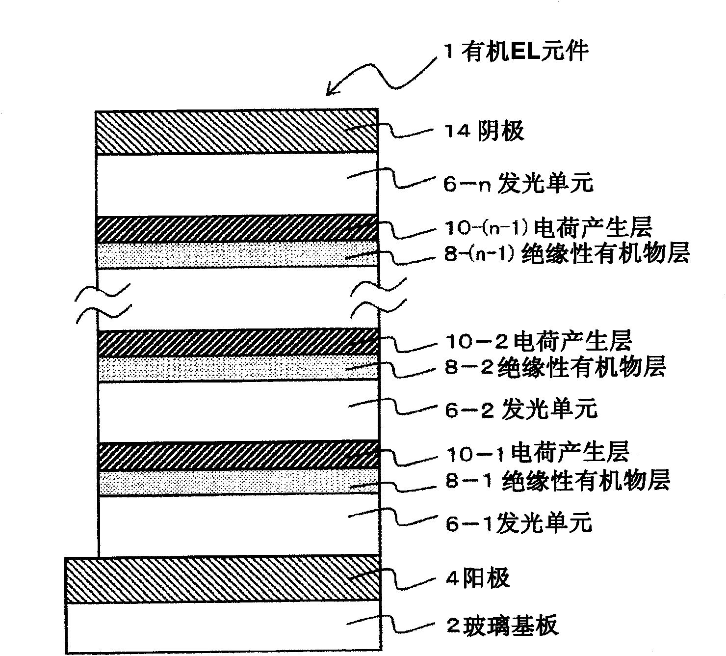
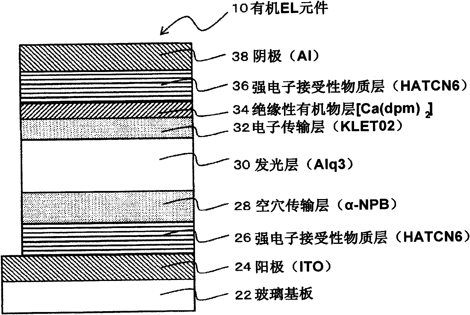
[0159] As the organic EL element of Example 1, the layer described below was sequentially stacked, which had figure 1 An organic EL element 1 of the structure shown. The constituent materials and thickness of each layer are as follows.
[0160] 1) Anode
[0161] ITO (Indium Tin Oxide), 800 Angstroms
[0162] 2) Strong electron-accepting material layer
[0163] HATCN6 (hexaazatriphenylene derivative), 200 Angstroms
[0164] 3) Hole transport layer
[0165] NPB{4,4′-bis[N-(2-naphthyl)-N-anilino]biphenyl}, 500 Angstroms
[0166] 4) Light-emitting layer
[0167] Alq3 [tris(8-hydroxyquinoline) aluminum complex], 300 Angstroms
[0168] 5) Electron transport layer
[0169] KLET02 manufactured by CHEMIPRO KASEI KAISHA, LTD., Japan, 250 Angstroms
[0170] 6) Insulating organic layer
[0171] Ca(dpm) 2 [bis(2,2,6,6-tetramethyl-3,5-heptanedionate) calcium], 60 Angstroms
[0172] 7) Strong electron-accepting material layer
[0173] HATCN6 (hexaazatriphenylene derivative), 200...
Embodiment 2
[0225] As the organic EL element of Example 2, an organic EL element having a structure in which the layers described below were sequentially laminated on a glass substrate was produced.
[0226] 1) Anode
[0227] ITO (Indium Tin Oxide), 800 Angstroms
[0228] 2) Strong electron-accepting material layer
[0229] HATCN6 (hexaazatriphenylene derivative), 200 Angstroms
[0230] 3) Hole transport layer
[0231] NPB{4,4′-bis[N-(2-naphthyl)-N-anilino]biphenyl}, 500 Angstroms
[0232] 4) Light-emitting layer
[0233] Alq3 [tris(8-hydroxyquinoline) aluminum complex], 200 Angstroms
[0234] 5) Electron transport layer
[0235] KLET02 manufactured by CHEMIPRO KASEI KAISHA, LTD., Japan, 250 Angstroms
[0236] 6) Insulating organic layer (hole-transporting organic layer, a layer that functions as an insulating layer on the electron-transporting site)
[0237] NPB{4,4′-bis[N-(2-naphthyl)-N-anilino]biphenyl}, 60 Angstroms
[0238] 7) Strong electron-accepting material layer
[023...
Embodiment 3
[0262] As the organic EL element of Example 3, an organic EL element having two light-emitting layers, that is, two light-emitting units, was fabricated by sequentially laminating the layers described below on a glass substrate.
[0263] 1) Anode
[0264] ITO (Indium Tin Oxide), 800 Angstroms
[0265] 2) Strong electron-accepting material layer
[0266] HATCN6 (hexaazatriphenylene derivative), 200 Angstroms
[0267] 3) The hole transport layer of the first light-emitting unit
[0268] NPB{4,4′-bis[N-(2-naphthyl)-N-anilino]biphenyl}, 500 Angstroms
[0269] 4) The light-emitting layer of the first light-emitting unit
[0270] Alq3 [tris(8-hydroxyquinoline) aluminum complex], 200 Angstroms
[0271] 5) The electron transport layer of the first light-emitting unit
[0272] KLET02 manufactured by CHEMIPRO KASEI KAISHA, LTD., Japan, 250 Angstroms
[0273] 6) Insulating organic layer (hole-transporting organic layer, a layer that functions as an insulating layer on the electron...
PUM
 Abstract
Description
Claims
Application Information