Hall element of two-dimensional electronic gas structure and manufacturing method thereof

A two-dimensional electron gas and Hall element technology, which is applied in the manufacture/processing of Hall effect devices, parts of electromagnetic equipment, and electromagnetic devices, can solve the problem of failure to work normally, low sensitivity, and failure to work at high temperatures and other issues to achieve the optimal effect of area utilization

Inactive Publication Date: 2012-04-04
INST OF MICROELECTRONICS CHINESE ACAD OF SCI
View PDF4 Cites 11 Cited by
  • Summary
  • Abstract
  • Description
  • Claims
  • Application Information

AI Technical Summary

Problems solved by technology

Among them, the silicon material Hall element is cheap and can be well compatible with integrated circuits, but its disadvantage is that the sensitivity is not high and it cannot work at high temperature.
Compound material Hall elements have great advantages in making high-sensitivity de

Method used


Image

  • Hall element of two-dimensional electronic gas structure and manufacturing method thereof
  • Hall element of two-dimensional electronic gas structure and manufacturing method thereof
  • Hall element of two-dimensional electronic gas structure and manufacturing method thereof

Examples


preparation example Construction

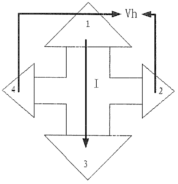
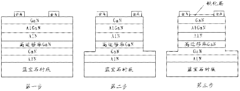
[0029] based on figure 2 As shown in the Hall element of the two-dimensional electron gas structure, the present invention also provides a preparation method of the Hall element of the two-dimensional electron gas structure, the method comprising: making an ohmic contact metal on the epitaxial material structure; performing mesa etching on the epitaxial material structure of the ohmic contact metal; and performing surface passivation on the epitaxial material structure performing mesa etching. The specific preparation process is as image 3 shown.

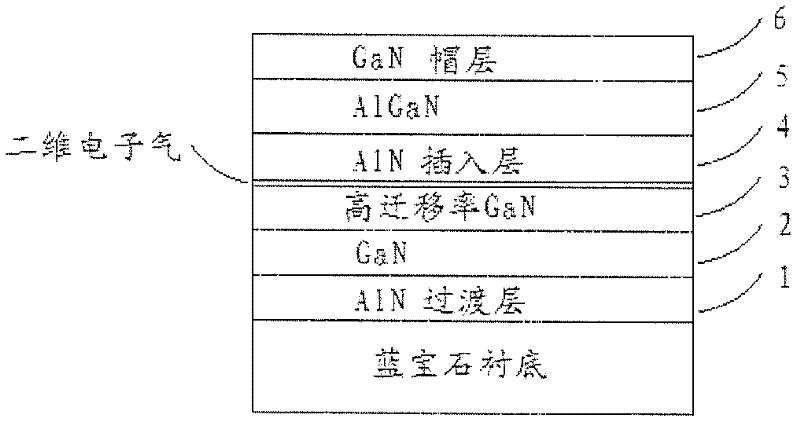
[0030] exist image 3In the step of making ohmic contact metal (i.e. the first step), the epitaxial material structure is a two-dimensional electron gas multilayer composite structure grown on a sapphire substrate, and the two-dimensional electron gas multilayer composite structure is included in The AlN transition layer, GaN layer, high-mobility GaN layer, AlN insertion layer, AlGaN layer and GaN cap layer grown sequentially o...

Embodiment

[0036] 1) Epitaxial growth of GaN / AlN / AlGaN two-dimensional electron gas Hall element materials.

[0037] Epitaxial material growth uses the method of MOCVD (Metal Organic Chemical Vapor Deposition). First, the first epitaxial layer on the sapphire substrate is an AlN transition layer with a thickness of 100nm; then grow GaN and high-mobility GaN layers with a thickness of 2μm and 100nm respectively, and grow the fourth layer as an AlN transition layer with a thickness of 0.7nm, followed by The fifth layer of growth is AlGaN with a thickness of 22nm, and the sixth layer is a GaN cap layer with a thickness of 2nm. At this point, the growth of the material is over.

[0038] 2) Preparation process of GaN / AlN / AlGaN two-dimensional electron gas Hall element.

[0039] In the first step, make the ohmic contact metal. The substrate was subjected to standard cleaning, and then dried in a 120-degree oven for 10 minutes. Using inversion photoresist AZ5214E, ohmic contact metal was fa...


PUM

PropertyMeasurementUnit
Thicknessaaaaaaaaaa
Thicknessaaaaaaaaaa
Thicknessaaaaaaaaaa

Abstract

The invention, relating to the technical field of a hall element, discloses the hall element of a sapphire substrate GaN/AlN/AlGaN two-dimensional electronic gas structure and a manufacturing method thereof, as well as an epitaxial material structure of the hall element of the two-dimensional electronic gas structure. The hall element disclosed by the invention can work at extreme temperatures such as above 300 degrees centigrade and below -50 degrees centigrade and the like. Meanwhile, an optimal design of area utilization rate is proposed for miniaturization and batch production. Finally technological process for manufacturing the hall element is provided. The sensitivity of the hall element can reach 7.28mV/mA*KGs through a sensitivity test. The hall element structure and the preparation method provided by the invention also can be applied to the preparation of hall elements of other substrate materials.

Description

technical field [0001] The present invention relates to the technical field of Hall elements, in particular to a Hall element with a GaN / AlN / AlGaN two-dimensional electron gas structure on a sapphire substrate and a preparation method thereof, and an epitaxial material structure for the Hall element with a two-dimensional electron gas structure . Background technique [0002] Hall element is currently one of the most widely used magnetic sensitive elements, widely used in automotive electronics, precision measurement, household electronics, industrial control and other fields. [0003] Among the mature Hall elements currently on the market, the most widely used are silicon material Hall elements and compound material Hall elements. Among them, the silicon material Hall element is cheap and can be well compatible with integrated circuits, but its disadvantage is that its sensitivity is not high and it cannot work at high temperature. Compound material Hall elements have gre...

Claims


Application Information

Patent Timeline
IPC IPC(8): H01L43/10H01L43/04H01L43/06H01L43/14
Inventor 李博刘洪刚刘新宇
Owner INST OF MICROELECTRONICS CHINESE ACAD OF SCI
Why Eureka
Try Eureka