Manufacturing method of field blocking type semiconductor device

A production method and field blocking technology, which is applied in semiconductor/solid-state device manufacturing, electrical components, circuits, etc., can solve the problems of high cost, not higher than 500 degrees Celsius, and low ion efficiency of the field blocking layer, reaching the depth range Large and good activation rate, impurity concentration and concentration distribution adjustable effect

Active Publication Date: 2012-04-11
SHANGHAI HUAHONG GRACE SEMICON MFG CORP
View PDF5 Cites 2 Cited by
  • Summary
  • Abstract
  • Description
  • Claims
  • Application Information

AI Technical Summary

Problems solved by technology

The other is to perform ion implantation of N-type impurities such as phosphorus or arsenic on the back of the device after the front process is completed, and then activate it by annealing. This annealing includes ordinary high-temperature annealing and laser annealing; The annealing temperature generally cannot be higher than 500 degrees Celsius when using ordinary annealing technology, and the efficiency of the implanted field-blocking layer ions is not activated; and the use of laser annealing can greatly improve the efficiency but the cost is very high

Method used


Image

  • Manufacturing method of field blocking type semiconductor device
  • Manufacturing method of field blocking type semiconductor device
  • Manufacturing method of field blocking type semiconductor device

Examples


Embodiment Construction

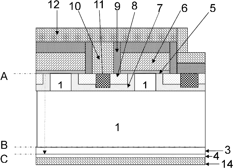
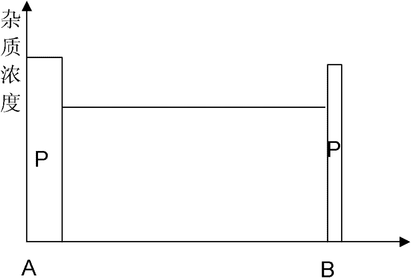
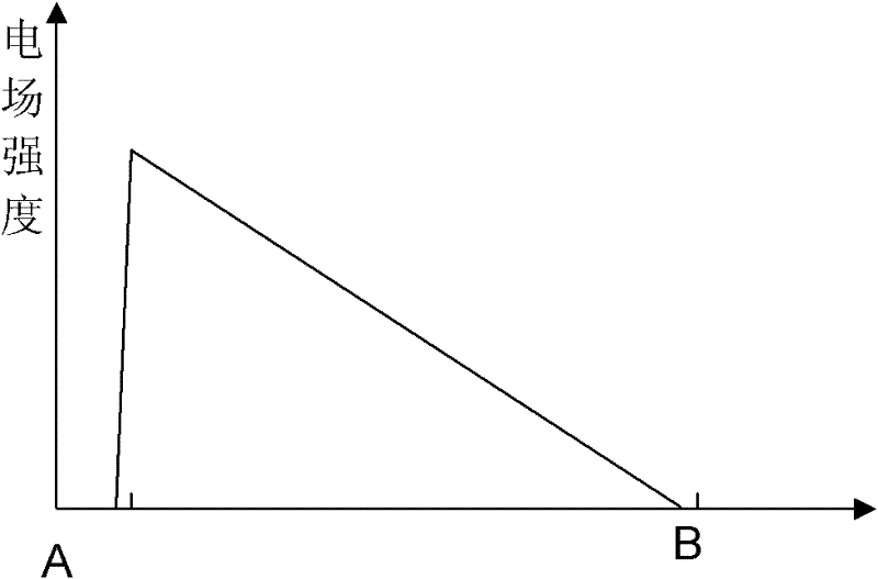
[0036] Such as Figure 6 Shown is a flow chart of a method for fabricating a field-stop type semiconductor device according to an embodiment of the present invention. The field-stop type semiconductor device in Embodiment 1 of the present invention is illustrated by taking a field-stop type IGBT device with a reverse breakdown voltage of 3300V and an N-type drift region as an example. The field-stop type IGBT with an N-type drift region The first conductivity type of the device is N-type; the method for manufacturing a field-blocking semiconductor device according to the embodiment of the present invention includes the following steps:

[0037] Step 1, such as Figure 7 As shown, first provide an impurity concentration C1 = 2.4E13CM -3 1. An N-type silicon chip 1 with a resistivity of 180 ohm.cm, the thickness of the silicon chip 1 is more than 700 microns; an oxide film of 5000 angstroms to 20000 angstroms is grown on the front side of the silicon chip 1, that is, on the se...


PUM


Abstract

The invention discloses a manufacturing method of a field blocking type semiconductor device. The method disclosed by the invention is characterized in that: a manufacturing process of a field blocking layer is advanced before other device manufacturing processes such as device front processes, so that when the field blocking layer is formed, even if a high-temperature process is adopted, the influence on other device processes such as metal materials can be avoided. Thus, the flexibility and adjustability of the field blocking layer forming process can be improved, and the field blocking layer with a large depth range, adjustable impurity concentration and concentration distribution and high activation rate can be formed. In addition, the method disclosed by the invention has no need of adopting a laser annealing process with high cost, thus lowering the cost.

Description

technical field [0001] The invention relates to a manufacturing process method of a semiconductor integrated circuit, in particular to a manufacturing method of a field-blocking type semiconductor device. Background technique [0002] In semiconductor high-voltage devices, whether it is an insulated gate bipolar transistor (IGBT), a fast recovery diode (FRD), or a MOSFET, when the gate of the device is positively biased, the device is turned on. The power consumption is the smallest, that is, the on-state voltage drop of the device is expected to be small, and the on-state voltage drop of the device can be directly reduced by using a thinner silicon chip, but the decrease in the thickness of the device will reduce the reverse breakdown of the device. Under the condition of pressure resistance, the two are a pair of contradictions. In order to solve the above contradictions, the field blocking layer is introduced into the semiconductor high-voltage device to form a field blo...

Claims


Application Information

Patent Timeline
Patent Type & Authority Applications(China)
IPC IPC(8): H01L21/331H01L21/22H01L21/265
Inventor 肖胜安
Owner SHANGHAI HUAHONG GRACE SEMICON MFG CORP
Why Eureka
Try Eureka