Surface treatment method for improving copper interconnection reliability

A surface treatment and reliability technology, applied in the direction of electrical components, semiconductor/solid-state device manufacturing, circuits, etc., to achieve the effect of improving bonding force, reducing damage, and improving overall performance

Active Publication Date: 2015-04-08
SHANGHAI HUALI MICROELECTRONICS CORP
View PDF7 Cites 0 Cited by
  • Summary
  • Abstract
  • Description
  • Claims
  • Application Information

AI Technical Summary

Problems solved by technology

[0007] In order to overcome the problems caused by the surface treatment technology in the process of manufacturing metal interconnection in the existing semiconductor manufacturing field, the present invention provides a surface that can improve the reliability of metal interconnection and reduce the damage increase of dielectric constant Approach

Method used


Image

  • Surface treatment method for improving copper interconnection reliability
  • Surface treatment method for improving copper interconnection reliability
  • Surface treatment method for improving copper interconnection reliability

Examples


Embodiment Construction

[0034] The present invention will be further described below with reference to the accompanying drawings and specific embodiments, but it is not intended to limit the present invention.

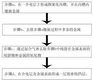
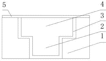
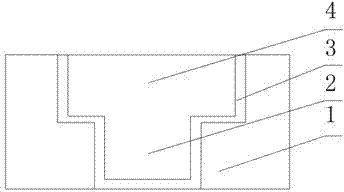
[0035] like figure 1 As shown, a surface treatment method for improving the reliability of copper interconnection of the present invention includes the following steps: figure 2 As shown, step a forms a photoresist material layer on the surface of the low-k dielectric layer 1 formed by chemical vapor deposition or spin coating; forms a predetermined pattern on the photoresist material layer by photolithography; uses the pattern The photoresist material layer is etched on the dielectric layer to form patterned trenches 2 , and the formed patterned trenches 2 may be a single-layer damascene structure or a double-layered damascene structure. A composite structure 3 composed of an adhesion layer, a diffusion barrier layer and a metal seed layer is sequentially formed on the sidewall and bottom ...


PUM


Abstract

The invention discloses a surface treatment method for improving copper interconnection reliability. The surface treatment method comprises the following steps of: a. forming a patterned groove on a dielectric layer and embedding metal in the patterned groove; b. removing residual metal in the embedding process in the step a; and c. removing residues and metal oxides on the surface by mixed gas. The invention has the benefits that oxides on the surface of a copper metal layer and residues in the chemical mechanical polishing process can be removed, thereby an atomic-scale cleaning surface is obtained; in addition, the bonding force of the cleaning surface and a nitride-containing barrier layer on the lower layer of the cleaning surface is improved, so that the copper interconnected electromigration resistant performance is improved, the stress resistant performance is improved and the dielectric breakdown life of a dielectric layer is prolonged; meanwhile, the damage to the dielectric layer in the prior art can be reduced and the improvement on the integrated performance of a chip is facilitated.

Description

technical field [0001] The invention relates to a surface treatment method, in particular to a surface treatment method for improving the reliability of copper interconnection in the process of manufacturing metal interconnection lines in the field of semiconductor manufacturing. Background technique [0002] In the semiconductor integrated circuit industry, high-performance integrated circuit chips require the lowest possible wiring capacitance, resistance, signal delay and signal crosstalk. For this reason, low-resistivity copper metal lines and the interlayer and inter-line filling of low-k dielectric materials are required to reduce parasitic capacitance and improve device performance. The low dielectric constant insulating dielectric material commonly used at present is carbon-doped porous silicon oxide. With the continuous reduction of dielectric constant requirements, the porosity and carbon content of dielectric materials continue to increase, and the structure beco...

Claims


Application Information

Patent Timeline
Patent Type & Authority Patents(China)
IPC IPC(8): H01L21/768
Inventor 张亮姬峰胡友存李磊陈玉文
Owner SHANGHAI HUALI MICROELECTRONICS CORP
Why Eureka
Try Eureka