Method for improving writing speed of floating body effect storage unit, and floating body effect storage unit

A memory cell and floating body effect technology, which is applied in the manufacture of transistors, electrical components, semiconductors/solid-state devices, etc., can solve problems such as leakage and needs to be improved, and achieve the goals of reducing leakage speed, increasing writing speed, and increasing substrate current Effect

Inactive Publication Date: 2012-05-02
SHANGHAI HUALI MICROELECTRONICS CORP
View PDF3 Cites 4 Cited by
  • Summary
  • Abstract
  • Description
  • Claims
  • Application Information

AI Technical Summary

Problems solved by technology

[0005] When the floating body effect memory cell is writing "1", the carriers will accumulate in the substrate while slowly leaking from the source. The inventor believes that the writing speed of the floating body effect memory cell ("1") has yet to be reached improve

Method used


Image

  • Method for improving writing speed of floating body effect storage unit, and floating body effect storage unit
  • Method for improving writing speed of floating body effect storage unit, and floating body effect storage unit
  • Method for improving writing speed of floating body effect storage unit, and floating body effect storage unit

Examples


Embodiment Construction

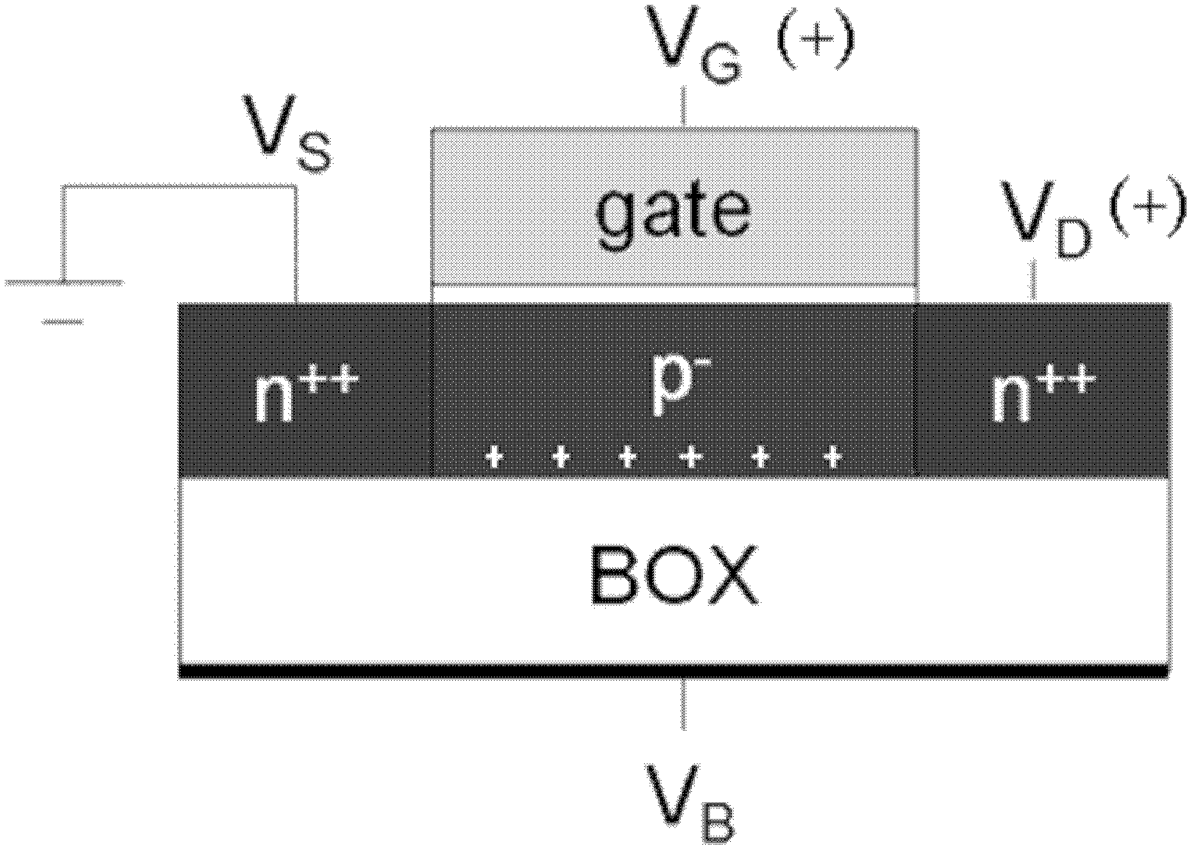
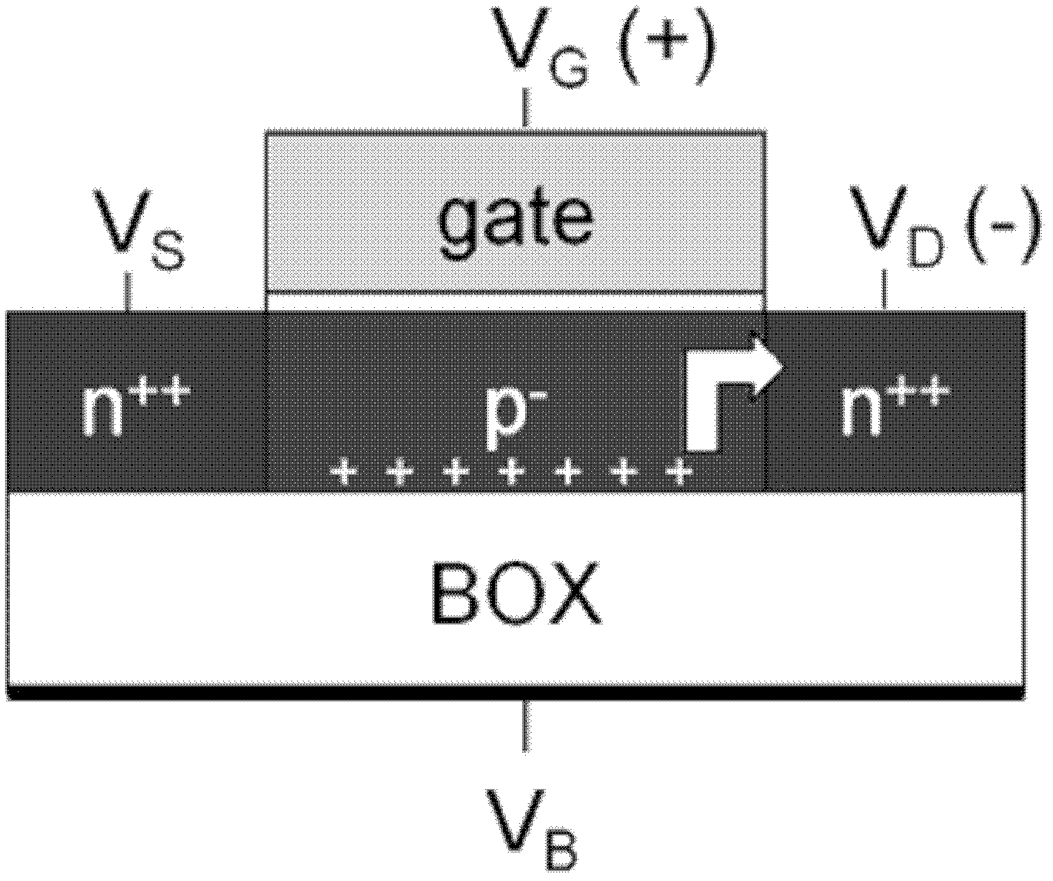
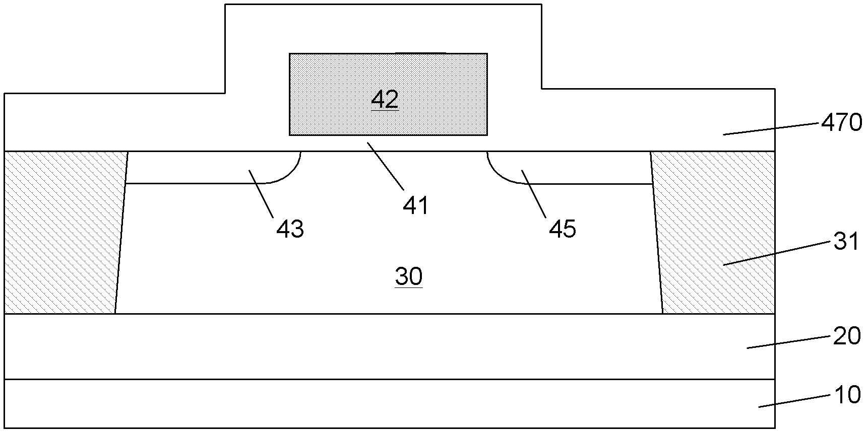
[0019] In the usual process, the sidewall formation (deposition and etching) process of the floating body effect memory cell is as follows: Figure 2A-2C shown.

[0020] First, the sidewall material is deposited, and the cross-section of the device after deposition is as follows Figure 2A shown. The floating body effect memory unit in the figure comprises bottom silicon 10, and described bottom silicon 10 is silicon-on-insulator for example; Formed on bottom silicon 10 Buried oxide layer 20; Formed on the substrate 30 of buried oxide layer 20, described The substrate 30 can be a silicon substrate, of course, in some occasions, a germanium substrate, a silicon germanium substrate or other semiconductor materials can also be applied; the shallow trench isolation groove 31 (shallow trench isolation, That is, STI), used to isolate each floating body effect memory cell; a gate oxide layer 41 and a gate 42 formed sequentially on the substrate 30, and a channel in the substrate 30...


PUM


Abstract

The invention provides a manufacturing method for improving the writing speed of a floating body effect storage unit, and the floating body effect storage unit, and belongs to the technical field of semiconductor manufacturing. The invention adopts the core scheme that: a mask layer is formed on a sidewall material which is adjacent to a source, and the sidewall material which is adjacent to a drain is exposed; partial thickness of the exposed sidewall material is etched; the mask layer is removed, and the sidewall material is re-etched, sidewalls are formed on two sides of a gate, and the sidewall which is adjacent to the source is wider than the sidewall which is adjacent to the drain; and by using the sidewalls as masks, heavy doping and annealing processes are performed to form the source and the drain, doped ions of the drain are closer to a channel, and the doped ions of the source are closer to the channel and a substrate. By the invention, a longitudinal electric field in the channel of the drain is improved, and the current of the substrate is improved; moreover, the leakage speed of accumulation carriers from the source is reduced, so that the writing speed of the floating body effect storage unit is improved.

Description

technical field [0001] The invention relates to the technical field of semiconductor manufacturing, in particular to a manufacturing method capable of increasing the writing speed of a floating body effect memory unit and the floating body effect memory unit, thereby improving the writing speed of a dynamic random access memory having the floating body effect memory unit . Background technique [0002] The development of embedded dynamic storage technology has made large-capacity dynamic random access memory (Dynamic Random Access Memory, DRAM) very common in current System on a Chip (SoC). Large-capacity embedded DRAM brings SoC benefits such as improved bandwidth and reduced power consumption that can only be achieved by using embedded technology. In addition to transistors, each storage unit of traditional embedded dynamic random access memory (embbeded Dynamic Random Access Memory, eDRAM) also needs a deep trench capacitor structure. The deep trench of the capacitor mak...

Claims


Application Information

Patent Timeline
Patent Type & Authority Applications(China)
IPC IPC(8): H01L21/8242H01L27/108
Inventor 俞柳江毛智彪
Owner SHANGHAI HUALI MICROELECTRONICS CORP
Why Eureka
Try Eureka