Method for boron doping of crystalline silicon solar battery

A technology of solar cells and boron doping, applied in the field of solar cells, can solve the problems of shortened service life of quartz furnace tubes, corrosion of quartz furnace tubes, etc., and achieves the effects of fast coating speed, low equipment cost, and extended service life.

Inactive Publication Date: 2012-05-02
JA SOLAR TECH YANGZHOU +1
View PDF6 Cites 21 Cited by
  • Summary
  • Abstract
  • Description
  • Claims
  • Application Information

AI Technical Summary

Problems solved by technology

At the same time BBr 3 It is also corrosive to quartz furnace tubes, which greatly shortens the service life of quartz furnace tubes

Method used


Image

  • Method for boron doping of crystalline silicon solar battery
  • Method for boron doping of crystalline silicon solar battery

Examples


Embodiment 1

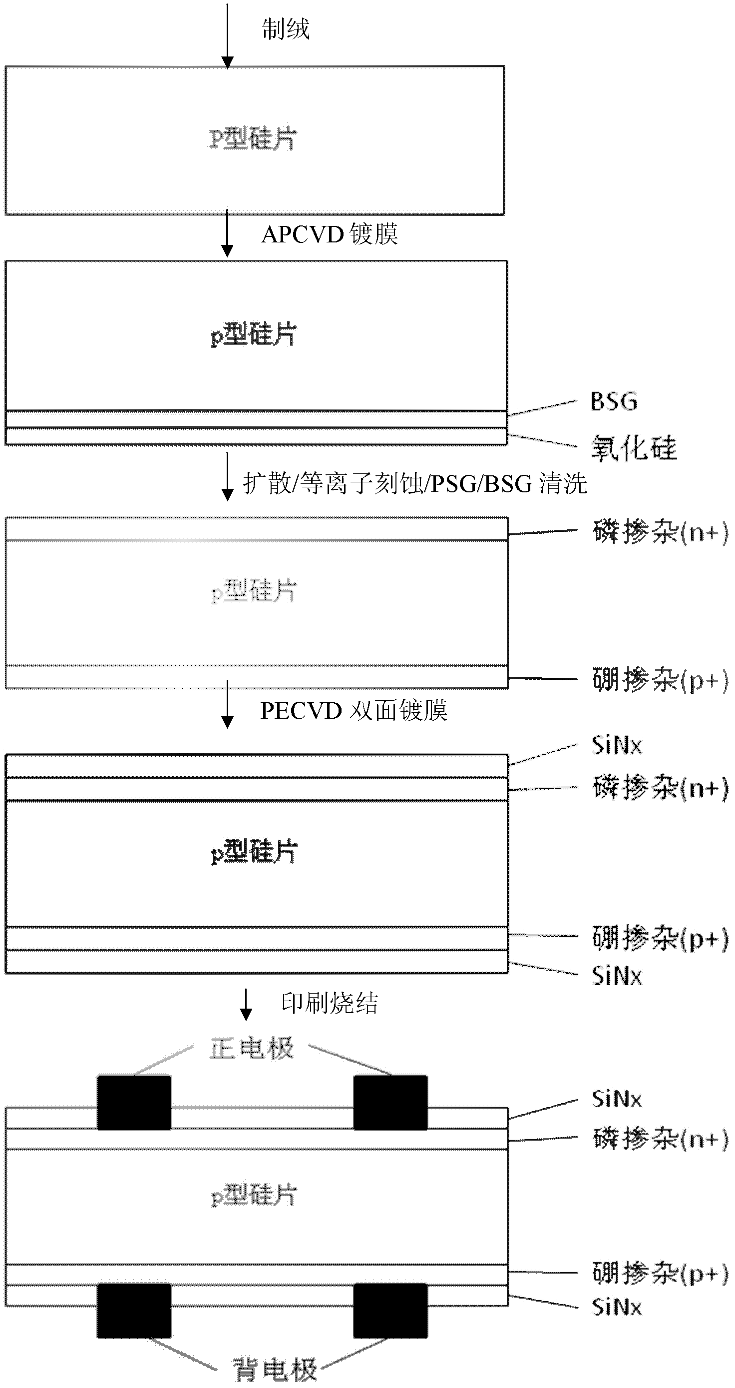
[0027] Utilize the boron doping method of the present invention to form a boron back field to prepare a p-type solar cell, such as figure 1 As shown in , this embodiment includes the following steps:

[0028] (1) Wafer selection, texturing and cleaning

[0029] Select a p-type monocrystalline silicon wafer, use 0.5-3% by weight of sodium hydroxide aqueous solution to make texture to obtain a pyramid-shaped texture, and then wash off the lye;

[0030] (2) Atmospheric pressure chemical vapor deposition method APCVD coating

[0031] Deposit BSG (boron-doped silicon oxide) on one side of the silicon wafer, and then deposit a second layer of silicon oxide on the BSG. The reaction atmosphere used in the atmospheric pressure chemical vapor deposition method is SiH 4 , O 2 , B 2 h 6 ; Wherein the film thickness of the first layer of film-boron-doped silicon oxide film is 100nm, and the concentration of boron in the boron-doped silicon oxide film is 10 22 / cm 3 ; The film thickn...

Embodiment 2

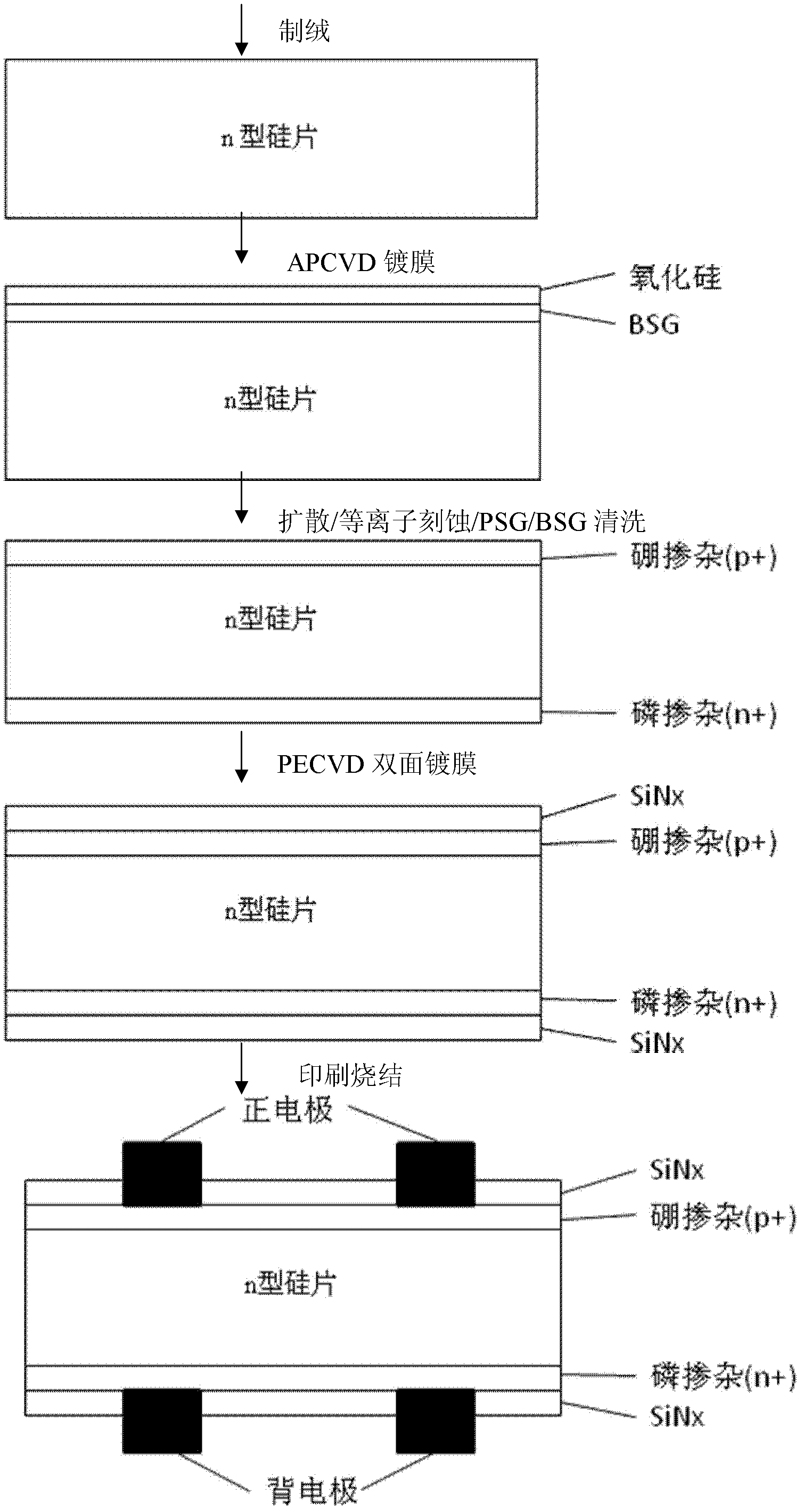
[0042] Utilize the boron doping method of the present invention to form a boron emitter to prepare an n-type solar cell, such as figure 2 As shown, this embodiment includes the following steps:

[0043] (1) Wafer selection, texturing and cleaning

[0044] Select n-type monocrystalline silicon wafers, use 0.5-3% by weight aqueous sodium hydroxide solution to make texture to obtain pyramid-shaped texture, and then wash off the lye;

[0045] (2) APCVD coating

[0046] Deposit BSG (boron-doped silicon oxide) on one side of the silicon wafer, and then deposit a second layer of silicon oxide on the BSG. The reaction atmosphere used in the atmospheric pressure chemical vapor deposition method is SiH 4 , O 2 , B 2 h 6 ; Wherein the film thickness of the first layer of film-boron-doped silicon oxide film is 100nm, and the concentration of boron in the boron-doped silicon oxide film is 10 22 / cm 3 The film thickness of the second film-silicon oxide film is 100nm;

[0047] (3) H...

Embodiment 3

[0057] (1) Wafer selection, texturing and cleaning

[0058] Select p-type polysilicon wafer, use HF and HNO 3 Mixing solutions to make suede;

[0059] (2) Atmospheric pressure chemical vapor deposition method APCVD coating

[0060] Deposit BSG (boron-doped silicon oxide) on one side of the silicon wafer, and then deposit a second layer of silicon oxide on the BSG. The reaction atmosphere used in the atmospheric pressure chemical vapor deposition method is SiH 4 , O 2 , B(CH 3 ) 3 ; The film thickness of the first layer of film-boron-doped silicon oxide film is 5nm, and the concentration of boron in the boron-doped silicon oxide film is 10 17 / cm 3 ; The film thickness of the second film-silicon oxide film is 5nm;

[0061] (3) High temperature diffusion

[0062] The boron-doped silicon oxide film and the silicon oxide film double-layer film deposited by the normal pressure chemical vapor deposition method APCVD are used as the barrier layer, the silicon wafer is placed ...


PUM

PropertyMeasurementUnit
thicknessaaaaaaaaaa
thicknessaaaaaaaaaa
thicknessaaaaaaaaaa

Abstract

The invention discloses a method for boron doping of a crystalline silicon solar battery, which comprises the following steps that: a first layer of film-boron doped silicon oxide film is deposited on the surface of a silicon chip after the wool making, a second layer of film-silicon oxide film is deposited on the first layer of the film to be used as a barrier layer, then the silicon chip is processed at high temperature, so boron atoms can be diffused into a silicon basic body to form a boron doped layer. Due to the adoption of the method, a boron transmission electrode (p+) can be prepared on an n-type silicon chip, or a boron back surface (p+) is formed on a p-type silicon chip. Through the barrier layer, single-faced boron doping can be realized, and a boron source is free from being sucked into a diffusion furnace tube, so the corrosion of the furnace tube can be reduced, and the service life can be prolonged; and if a phosphorus source is introduced during the high-temperature annealing process, the boron doping and phosphorus doping can be respectively realized on two sides of the silicon chip.

Description

technical field [0001] The invention belongs to the technical field of solar cells, and in particular relates to a boron doping method for crystalline silicon solar cells. Background technique [0002] Crystalline silicon solar cells are currently the mainstream in the photovoltaic market due to their high conversion efficiency and long service life. Commercial mass-produced crystalline silicon cells are mainly p-type cells. The emitter (p-n junction) can be formed on the surface of crystalline silicon through phosphorus diffusion, and the aluminum back field of the p+ layer is obtained by sintering the aluminum paste and silicon. The manufacturing process is relatively simple and mature, but the room for improving the conversion efficiency is becoming smaller and smaller. Therefore, people turn their attention to p-type cells with other structures and cells using n-type silicon wafers as substrates with higher minority carrier life and lower light-induced attenuation. [...

Claims


Application Information

Patent Timeline
Patent Type & Authority Applications(China)
IPC IPC(8): H01L31/18
CPCY02P70/50
Inventor 尹海鹏徐礼张俊兵刘淑华乔柳杨玉杰单伟
Owner JA SOLAR TECH YANGZHOU
Why Eureka
Try Eureka