Supercharge Your Innovation With Domain-Expert AI Agents!

Semiconductor material with Cu2O nano bamboo shoot structure and preparation method thereof

A semiconductor and nanotechnology, applied in the field of Cu2O nanometer bamboo shoot-structured semiconductor materials and their preparation, can solve the problems of difficulty in preparing one-dimensional nanostructures, low success rate, few raw materials, etc., and achieves good adhesion, low cost, and raw materials. less effect

Inactive Publication Date: 2012-05-09
EAST CHINA NORMAL UNIVERSITY
View PDF4 Cites 2 Cited by
  • Summary
  • Abstract
  • Description
  • Claims
  • Application Information

AI Technical Summary

Problems solved by technology

In recent years, the research focus is mainly on Cu 2 The controlled growth of O morphology enables the preparation of large-scale production, but so far there are few methods that can be applied to large-scale production of characteristic morphology
One-dimensional semiconducting nanomaterials have great application potential in the fields of optics and electronics, but due to Cu 2 O is a cuprite structure, and the preparation of its one-dimensional nanostructure is difficult
[0004] The present invention solves the problem of one-dimensional Cu in the prior art 2 Due to the problems of high cost and low success rate in the preparation of O nanostructures, a Cu 2 A method for preparing a semiconductor material with a nano-bamboo shoot structure, which has the beneficial effects of less raw materials, low equipment requirements, low cost, and large output.

Method used


Image

  • Semiconductor material with Cu2O nano bamboo shoot structure and preparation method thereof
  • Semiconductor material with Cu2O nano bamboo shoot structure and preparation method thereof
  • Semiconductor material with Cu2O nano bamboo shoot structure and preparation method thereof

Examples


preparation example Construction

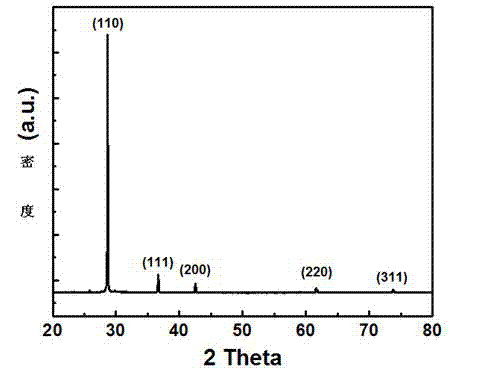
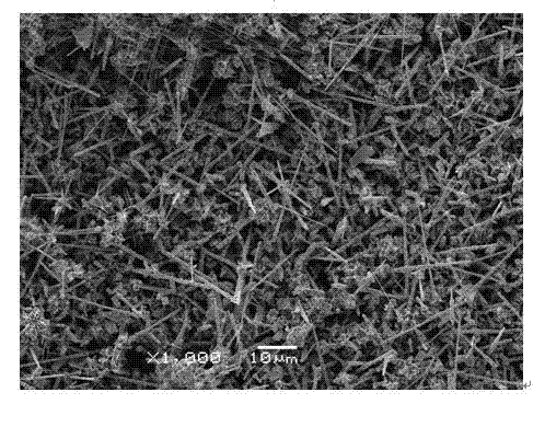
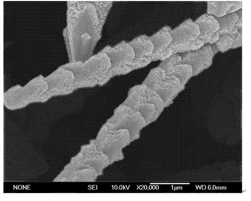
[0028] The present invention Cu 2 The preparation method of the semiconductor material of O nano shoot structure is to deposit Cu on the silicon chip 2 The preparation method of O nano shoot structure semiconductor material, comprises the steps:

[0029] a, absolute ethanol and deionized water are mixed in a certain volume ratio as a reaction solvent for use; a certain amount of Cu(CH 3 COO) 2 ·H 2 O and a small amount of pyrrole are added in the above solvent and stirred evenly to obtain the reaction solution;

[0030] b. Take a small piece of cleaned silicon wafer and put it into the bottom of the inner tank of the reaction kettle, and slowly add the above prepared reaction solution;

[0031] c. Put the sealed reaction kettle in a heating furnace heated to 180°C in advance to react for a period of time. The reaction temperature range of the preparation method of the present invention is 160-190°C.

[0032] d, after the reaction is over, take out the silicon chip covere...

Embodiment 1

[0036] 1. Clean the silicon wafer, and then cut it into small pieces of about 5mm×5mm;

[0037] 2. Set the temperature of the heating furnace to 180°C;

[0038] 3. Mix anhydrous ethanol and deionized water according to the volume ratio of 1:3 and stir evenly as a solvent for later use;

[0039] 4. Add Cu(CH 3 COO) 2 ·H 2 O powder was added to 100mL of the above-mentioned mixed solvent of absolute ethanol and deionized water to prepare Cu(CH 3 COO) 2 ·H 2 O content is the mixed solution of 25mM; Cu(CH 3 COO) 2 ·H 2 The O content allows an error of up and down 2.5mM, which has no effect on the reaction result;

[0040] 5. After stirring for about 5 minutes, add pyrrole dropwise to the above solution while stirring, Cu(CH 3 COO) 2 ·H 2 The molar ratio of O powder to pyrrole is 2:7, and the prepared reaction solution is light blue;

[0041] 6. Clean the Teflon reactor with a capacity of 100mL, place the cleaned silicon wafer horizontally on the bottom of the inner tan...


PUM


Abstract

The invention belongs to the technical fields of photoelectron materials, semiconductor materials and devices and discloses a semiconductor material with a Cu2O nano bamboo shoot structure. The semiconductor material comprises a silicon wafer and a Cu2O nano bamboo shoot structure crystal which is deposited on the silicon wafer, wherein the Cu2O nano bamboo shoot structure crystal comprises a nano rod and a periodically-layered branch Cu2O crystal which is derived from the nano rod. The invention further discloses a preparation method of the semiconductor material with the Cu2O nano bamboo shoot structure, which is prepared by mixing absolute ethyl alcohol and water to prepare a solvent serving as a solvent, taking Cu(CH3COO)2.H2O powder and pyrrole as raw materials, and utilizing a hydrothermal method. The preparation method provided by the invention has the advantages of large production volume, low cost, high repetitiveness and the like. The semiconductor material with the Cu2O nano bamboo shoot structure is special in shape and is good for limiting the transmission of electrons on one dimensionality by serving as the semiconductor material with a one-dimensional structure, so that the transmission efficiency is greatly improved and the semiconductor material has a good prospect on manufacturing a high-performance electronic device.

Description

technical field [0001] The invention belongs to the technical field of optoelectronic materials, semiconductor materials and devices, and in particular relates to a semiconductor material with Cu2O nano shoot structure and a preparation method thereof. Background technique [0002] Cu 2 O is a p-type semiconductor material with a direct bandgap of about 2.17eV, and has many unique electrical, optical and magnetic properties, so it is used in solar energy conversion, photocatalysis, sensors, antibacterial, lithium battery electrodes, etc. field has a wide range of applications. [0003] In the past few decades, people have prepared various Cu 2 O nanostructures, such as nanowires, cubes, octahedrons, dodecahedrons, hexahedrons, hollow spheres, etc., and various optoelectronic properties of these nanostructures have been studied. In recent years, the research focus is mainly on Cu 2 The controlled growth of O morphology can achieve large-scale production, but so far there ...

Claims


Application Information

Patent Timeline
IPC IPC(8): C04B41/50B82Y40/00
Inventor 石慧郁可朱自强
Owner EAST CHINA NORMAL UNIVERSITY
Features
  • R&D
  • Intellectual Property
  • Life Sciences
  • Materials
  • Tech Scout
  • Unparalleled Data Quality
  • Higher Quality Content
  • 60% Fewer Hallucinations
Learn More