
Method for forming nickel silicide with microwave annealing

A nickel silicide, microwave annealing technology, applied in electrical components, semiconductor/solid-state device manufacturing, semiconductor devices, etc., can solve problems such as the annealing time should not be too long, the temperature should not be too high, and the uniformity of nickel silicide is not very good. Achieving the effect of promoting rearrangement, improving performance, and improving uniformity

Inactive Publication Date: 2012-05-09
SHANGHAI HUALI MICROELECTRONICS CORP
View PDF1 Cites 8 Cited by
  • Summary
  • Abstract
  • Description
  • Claims
  • Application Information

AI Technical Summary

Problems solved by technology

In the traditional method, through two traditional thermal annealing, the annealing time should not be too long, and the temperature should not be too high, and the uniformity of the formed nickel silicide is not very good

Method used


Image

  • Method for forming nickel silicide with microwave annealing
  • Method for forming nickel silicide with microwave annealing
  • Method for forming nickel silicide with microwave annealing

Examples


Embodiment Construction

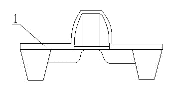
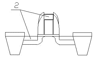
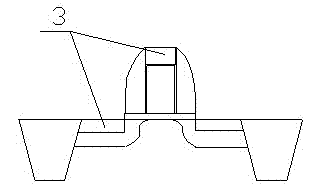
[0028] The present invention will be further described below in combination with principle diagrams and specific operation examples.

[0029] Such as image 3 Shown, the microwave annealing method of the present invention forms nickel silicide, wherein, comprises the following steps:

[0030] S1. Perform pre-cleaning on the exposed silicon surface to remove natural oxides; the step of pre-cleaning to remove natural oxides is completed by cleaning in a SiCoNi chamber or HF immersion, and removing a silicon surface layer with a thickness of 15A-50A. Nickel or nickel alloys are deposited on the cleaned silicon surface by physical vapor deposition.

[0031] S2. Deposit nickel or nickel alloy on the cleaned silicon surface, and cover a barrier layer on the surface of nickel or nickel alloy.

[0032] S3. During the process of heating the wafer to the first temperature, microwave radiation is used at the same time to make a part of nickel or nickel alloy react with silicon to form ...


PUM


Abstract

The invention discloses a method for forming nickel silicide with microwave annealing. The method comprises the following steps of: pre-cleaning the surface of exposed silicon for removing natural oxide; depositing nickel or nickel alloy and coating a layer of barrier layer on the surface of the nickel or nickel alloy; utilizing microwave radiation so that a part of the nickel or nickel alloy is reacted with the silicon to form high-resistance one-silication two-nickel in the process of heating a wafer to a first temperature at the same time; removing the barrier layer of the surface of the nickel or nickel alloy and unreacted nickel or nickel alloy; and utilizing microwave radiation so that the high-resistance one-silication two-nickel is changed to low-resistance nickle silicide in the process of heating the wafer to a second temperature at the same time. In the method, the surface of a silicon wafer is radiated by utilizing the microwave during heating at the same time, therefore, the activity of atomic motion is improved, and atomic realignment is promoted. The first temperature for heating is reduced so that the first step of diffusion of nickel is limited. The activity of the atomic motion is improved on the basis of the second temperature, therefore, the atomic realignment is promoted, the uniformity of the nickle silicide is helped to be improved, and the performance of devices is improved.

Description

technical field [0001] The invention relates to the technical field of semiconductor integrated circuit and its manufacture, in particular to a method for forming nickel silicide by microwave annealing. Background technique [0002] As the integration of semiconductor devices continues to increase and the critical dimensions associated with these devices continue to decrease, how to manufacture semiconductor devices with low-resistance materials to maintain or reduce signal delay has become the focus of attention, while the gate conductors and The reduction of the sheet resistance and contact resistance of the source / drain region is equally important as the subsequent interconnection. Silicide and salicide materials and processes have been widely used to reduce the sheet resistance and contact resistance of gate conductors and source / drain regions of CMOS devices. [0003] Metals and alloys including titanium, cobalt and nickel have been used to form silicide layers on semi...

Claims


Application Information

Patent Timeline
Patent Type & Authority Applications(China)
IPC IPC(8): H01L21/28H01L21/768
Inventor 周军
Owner SHANGHAI HUALI MICROELECTRONICS CORP
Learn More