Method and structure for enhancing write-in speed of floating body dynamic random memory cell

A technology of dynamic random access storage and writing speed, applied in semiconductor/solid-state device manufacturing, electrical components, semiconductor devices, etc., can solve the problems of incompatibility, difficult manufacturing process, limited application, etc. Writing speed, the effect of increasing the longitudinal electric field

Inactive Publication Date: 2012-05-09
SHANGHAI HUALI MICROELECTRONICS CORP
View PDF4 Cites 6 Cited by
  • Summary
  • Abstract
  • Description
  • Claims
  • Application Information

AI Technical Summary

Problems solved by technology

In addition to transistors, each storage unit of traditional embedded dynamic memory (eDRAM) also needs a deep trench capacitor structure. The deep trench of the capacitor makes the height of the storage unit much larger than its width, which makes the manufacturing process difficult
Its manufacturing process is very incompatible with CMOS VLSI process, which limits its application in embedded system chip (SOC)

Method used


Image

  • Method and structure for enhancing write-in speed of floating body dynamic random memory cell
  • Method and structure for enhancing write-in speed of floating body dynamic random memory cell
  • Method and structure for enhancing write-in speed of floating body dynamic random memory cell

Examples


Embodiment Construction

[0025] The present invention will be further described below in combination with principle diagrams and specific operation examples.

[0026] As shown in Figure 1, a kind of method of the present invention improves the writing speed of floating body DRAM unit, and it comprises the following steps:

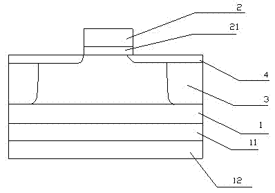
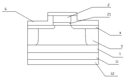
[0027] Such as Figure 1A As shown, gate 2 and shallow trench isolation trench 3 are prepared on substrate 1; lightly doped ions are implanted into substrate 1 and gate 2, and lightly doped sources are formed in the substrates on both sides of gate 2 drain 4;

[0028] In this step, the substrate 1 further includes a bottom layer 12 and an isolation layer 11 , wherein the isolation layer 11 is located between the bottom layer 12 and the substrate 1 . Preferably, the isolation layer 11 is a buried oxide layer, and the bottom layer 12 is made of silicon.

[0029] In addition, a thin oxide layer 21 is also included between the gate 2 and the substrate 1 .

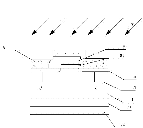
[0030] Such as Figure 1...


PUM


Abstract

The invention discloses a method for enhancing a write-in speed of a floating body dynamic random memory cell. A semiconductor device is manufactured on a substrate. and then the method also comprises the following steps that: ions are implanted into a side wall film layer at a certain angle alpha that is inclined to a drain region; the side wall film layer is etched; after the etching, the width of one portion of the side wall is larger than the width of the other portion of the side wall, wherein the one portion of the side wall is close to a source end and the other portion of the side wall is close to a drain end; and doping and annealing are carried out on the semiconductor device as well as a source electrode, a drain electrode and a channel are formed on the substrate. In addition, the invention also discloses a structure for enhancing a write-in speed of a floating body dynamic random memory cell. The structure comprises a substrate, a grid, and a shallow trench isolation channel. A side wall, which is covered on a side wall of the grid, includes a source end side wall and a drain end side wall, wherein the width of the source end side wall is greater than that of the drain end side wall. Besides, a source electrode, a drain electrode and a channel are formed on the substrate; and doped ions of the drain electrode are more close to the channel than doped ions of the source electrode to the channel.

Description

technical field [0001] The invention relates to a semiconductor preparation technology, in particular to an etching process method for forming an asymmetric side wall, which is used to improve the writing speed of a floating body effect memory unit. Background technique [0002] The development of embedded dynamic memory technology has made large-capacity DRAM very common in current system-on-chip (SOC). Large-capacity embedded dynamic memory (eDRAM) brings various benefits to SoCs such as improved bandwidth and reduced power consumption that can only be achieved by using embedded technology. In addition to transistors, each memory cell of traditional embedded dynamic memory (eDRAM) also needs a deep trench capacitor structure. The deep trench of the capacitor makes the height of the memory cell much larger than its width, which makes the manufacturing process difficult. Its manufacturing process is very incompatible with CMOS VLSI process, which limits its application in e...

Claims


Application Information

Patent Timeline
Patent Type & Authority Applications(China)
IPC IPC(8): H01L21/336H01L21/3115H01L21/311H01L29/78H01L29/08
Inventor 俞柳江
Owner SHANGHAI HUALI MICROELECTRONICS CORP
Why Eureka
Try Eureka