Copper foil with resistance layer, method of production of the same and laminated board

A technology of resistance layer and electrolytic copper foil, applied in directions including printed resistance, printed circuit manufacturing, coating, etc., can solve the problems of increasing dispersion and obtaining resistance value, and achieve the effect of small dispersion of resistance value

Inactive Publication Date: 2012-05-23
FURUKAWA ELECTRIC CO LTD
View PDF6 Cites 18 Cited by
  • Summary
  • Abstract
  • Description
  • Claims
  • Application Information

AI Technical Summary

Problems solved by technology

However, it is difficult to uniformly distribute the roughened particles on the surface of the copper foil through micro-roughening treatment. If the distribution of the roughened particles is not uniform, the thickness of the phosphorus-containing nickel electroplating thin film layer disposed on it (as a resistance element) will be reduced. Dispersion, the dispersion of each resistance value obtained in the in-plane resistance value measurement method specified in JIS-K-7194 becomes large, and there is a bad situation. Even if the resistance element pattern is formed in the circuit design, it may not be possible to obtain a theoretical value. resistance

Method used


Image

  • Copper foil with resistance layer, method of production of the same and laminated board
  • Copper foil with resistance layer, method of production of the same and laminated board
  • Copper foil with resistance layer, method of production of the same and laminated board

Examples


preparation example Construction

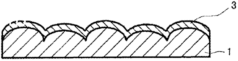
[0060] The reason for using a phosphorus-containing nickel bath in the preparation of the above-mentioned resistance layer 3 is that the bath conditions are easy to build and the resistance value of the resistance layer can be managed by controlling the amount of nickel adhesion and phosphorus content and their ratio, especially when using amino In the case of nickel sulfonate, since the remaining plating stress is small after forming a thin film, warpage can be suppressed, so it has advantages in both improved production efficiency and stable quality.

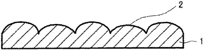
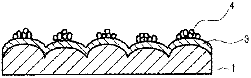
[0061] Here, the reason for using the rough side of the commonly used electrolytic copper foil to form the resistance layer is that if the rough surface shape is in the range of 2.5 to 6.5 μm in terms of Rz value, even if the thickness of the film reaches 250 Ω / □ in terms of resistance value The left and right electroplating thickness can also be plated without air pores. Even if the nickel rough treatment of nickels that attach ...

Embodiment 1

[0065] Using copper foil produced under the conditions of electrolytic foil production, the thickness of the copper foil is 18 μm, the shape roughness of the rough surface side (electrolyte surface side) is 4.8 μm Rz value specified in JIS-B-0601, and in The elongation after heating for 60 minutes at 180°C under atmospheric heating conditions was 14.2% (MP foil manufactured by Furukawa Electric Co., Ltd.). Roughening treatment and implementation of Capsur plating treatment.

[0066] [Bath Composition and Treatment Conditions for Forming Resistance Layer]

[0067] Use nickel sulfamate, calculated as nickel...65g / L

[0068] Phosphorous acid to PO 3 Count...40g / L

[0069] Hypophosphorous acid to PO 4 Count...50g / L

[0070] Boric acid (HBO 3 )......30g / L

[0071] pH: 1.6

[0072] Bath temperature: 55°C

[0073] Plating current density......5.0A / dm 2

[0074] [Nickel roughening treatment conditions]

[0075] Use nickel sulfate, calculated as nickel......18g / L

[0076] ...

Embodiment 2

[0092] In addition to using the following copper foil produced under the conditions of electrolytic foil production, it was processed under the conditions described in Example 1 and provided for evaluation and measurement; the thickness of the copper foil was 18 μm, and the shape roughness of the rough side was JIS- The Rz value specified in B-0601 is 4.5 μm, and the elongation after heating for 60 minutes at 180° C. under atmospheric heating conditions is 14.2% (MP foil manufactured by Furukawa Electric Co., Ltd.).

[0093] The measurement and evaluation results are also shown in Table 1.


PUM

PropertyMeasurementUnit
surface roughnessaaaaaaaaaa
thicknessaaaaaaaaaa
thicknessaaaaaaaaaa

Abstract

A copper foil with a resistance layer is provided, wherein the variation value is small when it is made into a resistance element, the adhesion with the resin substrate to be laminated with is able to be sufficiently maintained, which has an excellent characteristics as a resistance element for a rigid and a flexible substrate. A copper foil with a resistance layer of the present invention comprises a copper foil on one surface of which a metal layer or alloy layer is formed from which a resistance element is to be formed, the surface of the metal layer or alloy layer being subjected to a roughening treatment with nickel particles. A method of production of a copper foil with a resistance layer of the present invention comprises: forming a resistance layer of phosphorus-containing nickel on a matte surface of an electrodeposited copper foil having crystals comprised of columnar crystal grains wherein a foundation of the matte surface is within a range of 2.5 to 6.5 [mu]m in terms of Rz value prescribed in JIS-B-0601; and performing roughening treatment to a surface of the resistance layer with nickel particles wherein a roughness is within a range of 4.5 to 8.5 [mu]m in terms of Rz value prescribed in JIS-B-0601. The alloy layer is for example formed from phosphorus-containing nickel.

Description

technical field [0001] The present invention relates to a copper foil with a resistive layer and a preparation method thereof, and a laminated substrate using the copper foil with a resistive layer. The copper foil with a resistive layer can reduce the dispersion of resistance values ​​and has advantages as a resistive element for rigid substrates and flexible substrates. Excellent properties. Background technique [0002] In recent years, among electronic devices, portable electronic terminals represented by mobile phones have, on the basis of miniaturization and thinning, not only call functions, but also video and animation sending and receiving functions, and GPS (Global Positioning System) functions. , Single-band (one-seg) multi-functionality such as receiving signal function has also made remarkable progress. Along with this multi-functionalization, the modularization of the components of the portable terminal has also progressed by leaps and bounds. How to miniaturi...

Claims


Application Information

Patent Timeline
Patent Type & Authority Applications(China)
IPC IPC(8): C25D7/06C23C28/00C25D5/14H05K1/09
CPCC25D1/04H05K1/167C25D3/562C25D5/34H05K3/389H05K3/384C25D11/38C25D7/0628C25D5/48C23C30/00H05K2201/0355H05K2203/0307Y10T428/12076Y10T428/12049C25D5/617C25D5/605
Inventor 小黑了一加濑光路星野和弘
Owner FURUKAWA ELECTRIC CO LTD
Why Eureka
Try Eureka