Laser annealing method and laser annealing device adopting laser auxiliary heating

A laser annealing and auxiliary heating technology, which is applied in laser welding equipment, metal processing equipment, electrical components, etc., can solve the problems of inability to use laser annealing, inconvenient and flexible, etc., and achieve the goal of optimizing the laser annealing process, simplifying the process, and high annealing efficiency Effect

Active Publication Date: 2014-06-25
BEIJING ZK LASER
View PDF6 Cites 1 Cited by
  • Summary
  • Abstract
  • Description
  • Claims
  • Application Information

AI Technical Summary

Problems solved by technology

The disadvantage of this laser annealing method is that it cannot perform laser annealing on the specified area of ​​the semiconductor surface, which is not convenient and flexible enough.

Method used


Image

  • Laser annealing method and laser annealing device adopting laser auxiliary heating
  • Laser annealing method and laser annealing device adopting laser auxiliary heating
  • Laser annealing method and laser annealing device adopting laser auxiliary heating

Examples


Embodiment 1

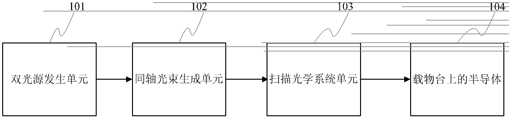
[0047] Such as Figure 1-b As shown, the present invention adopts a laser-assisted heating light source for coaxial transmission of the laser light source used for laser annealing, optimizes the activity of the surface of the semiconductor material to be annealed, and greatly improves the efficiency and effect of laser annealing. The method of the invention creates an original laser annealing scanning method in which the annealing light source performs laser annealing scanning in the horizontal and vertical directions on the surface of the semiconductor material, and changes the traditional laser annealing method in which the laser annealing light source is irradiated at a fixed point and the semiconductor material is rotated on the loading platform. The improved laser annealing method can realize laser annealing in a designated area on the semiconductor surface, which is a feature that traditional laser annealing equipment does not have. The technical solution adopted in the ...

Embodiment 2

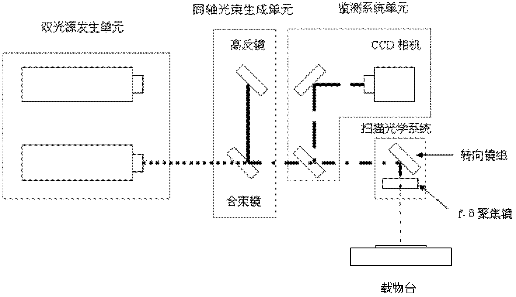
[0060] Such as Figure 5 As shown, this figure is one of the optional strategies for the co-optical axis transmission strategy described in the above method, specifically including:

[0061] Step 501, the laser beam used for auxiliary heating is turned and irradiated to the rear surface of the beam combining mirror through a high reflection mirror, and the rear surface of the beam combining mirror is coated with a high reflectivity film for the wavelength of the auxiliary heating laser, so that the auxiliary heating laser beam is once again Turn to transmission.

[0062] Step 502, the laser beam used for laser annealing is incident on the front surface of the beam combiner, and the front surface of the beam combiner is coated with a high transmittance film for the wavelength of the laser annealing laser, and the laser beam used for laser annealing passes through the beam combiner. The beam mirror continues to travel forward.

[0063] Step 503, adjusting the relative position...


PUM

PropertyMeasurementUnit
wavelengthaaaaaaaaaa

Abstract

The invention provides a laser annealing method and a laser annealing device adopting the laser auxiliary heating within the technical range of laser annealing in a semiconductor production process. The laser annealing method mainly adopts two lasers, wherein one laser is used for laser auxiliary heating to enable the surface of a semiconductor to be activated to make preparations for laser annealing, while the other one is used for laser annealing to the semiconductor. Two laser beams pass through a related optical system to be coaxially outputted and irradiated onto a scanning mirror. A scanning optical system is assembled on a precision mechanical component and is controlled electrically. An electric control system adopts a galvanometer control structure, and when the output voltage ranges from negative 10 V to positive 10 V, the mechanical structure deflects by 20 degrees below zero to 20 degrees correspondingly, so that the control to the input voltage is converted into the precision control to the turning angle of the mechanical structure. An optical lens is fixed on the mechanical structure, and the irradiation position of the laser beams is adjusted through controlling the turning angle of the scanning optical system, so that the laser beams are scanned in the horizontal direction and the vertical direction.

Description

technical field [0001] The invention relates to a semiconductor manufacturing equipment and method, in particular to a laser annealing method and device using laser assisted heating. Background technique [0002] Laser technology has achieved good application results in semiconductor production. Diffusion and impurity doping are performed using a laser process, the purpose of which is to obtain an abrupt junction that is not deposited deeply and to establish an ohmic contact. Laser annealing can electrically activate the implanted impurities and eliminate the radiation defects of the structure. It is also found that the laser can crystallize the silicon epitaxy and absorb the gas in the semiconductor structure. Another advantage of the laser annealing process is that no other products are generated during the annealing process. [0003] Based on most of the current laser annealing methods, a preheating process is added before the laser annealing process of the semiconducto...

Claims


Application Information

Patent Timeline
Patent Type & Authority Patents(China)
IPC IPC(8): B23K26/064B23K26/082B23K26/70H01L21/268B23K26/04
Inventor 彭海波彭俊刘全力
Owner BEIJING ZK LASER
Why Eureka
Try Eureka