
Conducting resin for scanning electronic microscope and preparation method thereof

An electron microscope and conductive resin technology, applied in the field of material processing, can solve problems such as high cost, sample surface damage, and inability to analyze samples chemically

Inactive Publication Date: 2013-11-06
BEIJING UNIV OF TECH
View PDF5 Cites 0 Cited by
  • Summary
  • Abstract
  • Description
  • Claims
  • Application Information

AI Technical Summary

Problems solved by technology

However, the gold film can prevent the incidence of X-rays, so the chemical analysis of the sample cannot be carried out with a scanning electron microscope.
In addition, the metal coating method is expensive and may cause damage to the sample surface

Method used


Image

  • Conducting resin for scanning electronic microscope and preparation method thereof
  • Conducting resin for scanning electronic microscope and preparation method thereof
  • Conducting resin for scanning electronic microscope and preparation method thereof

Examples


Embodiment 1

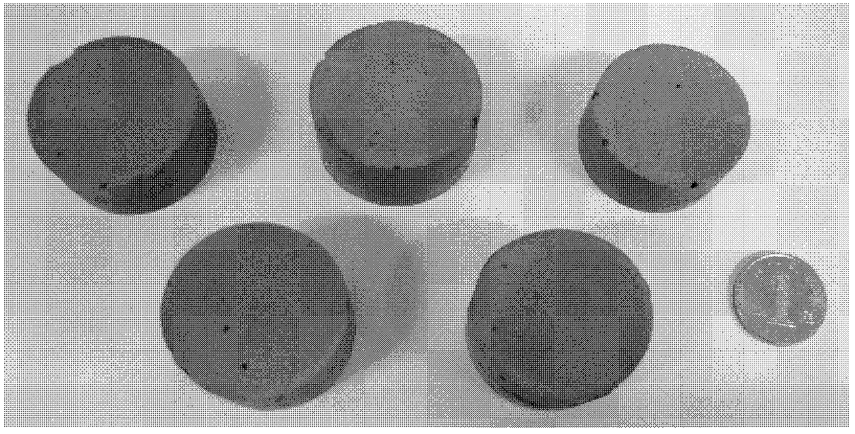
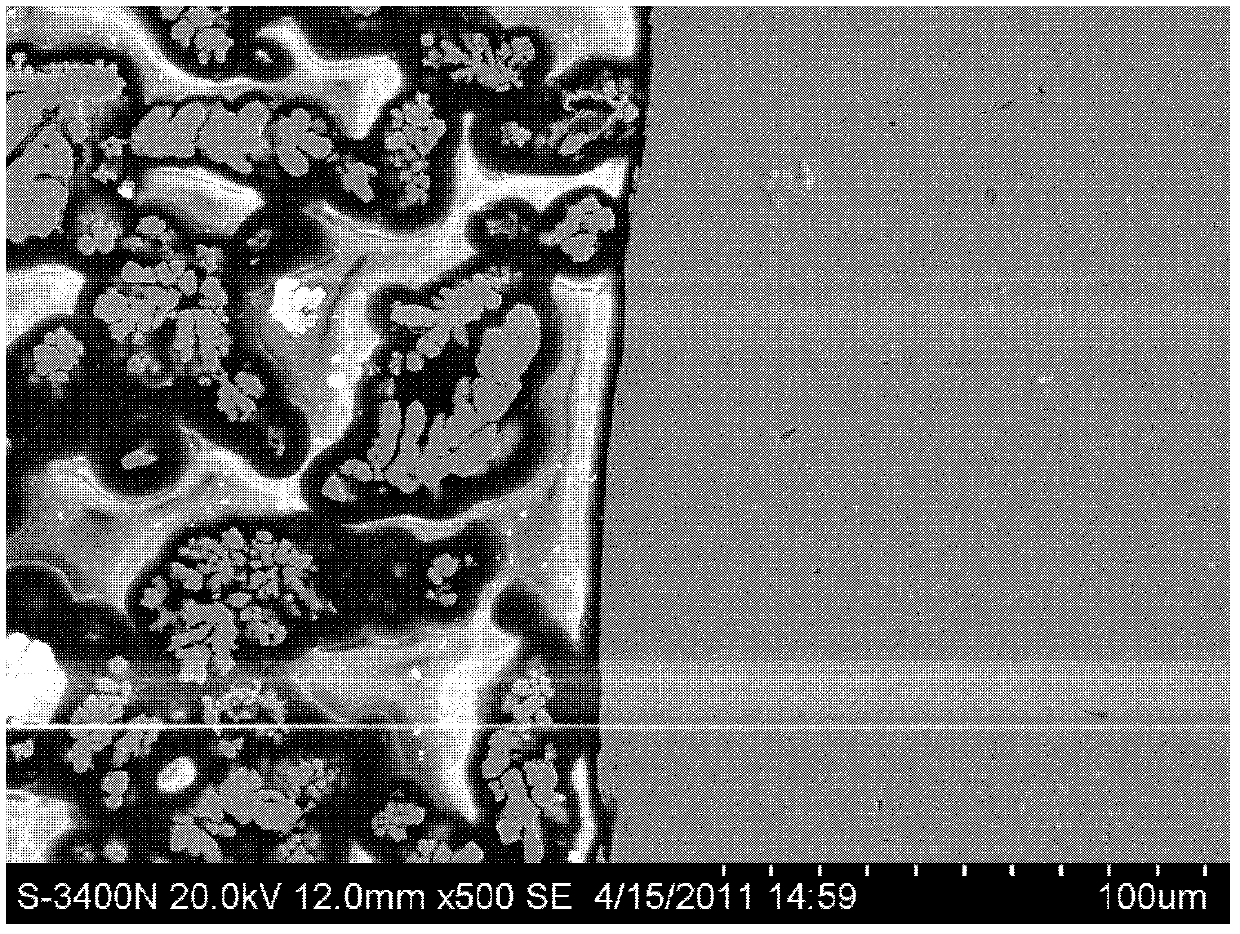
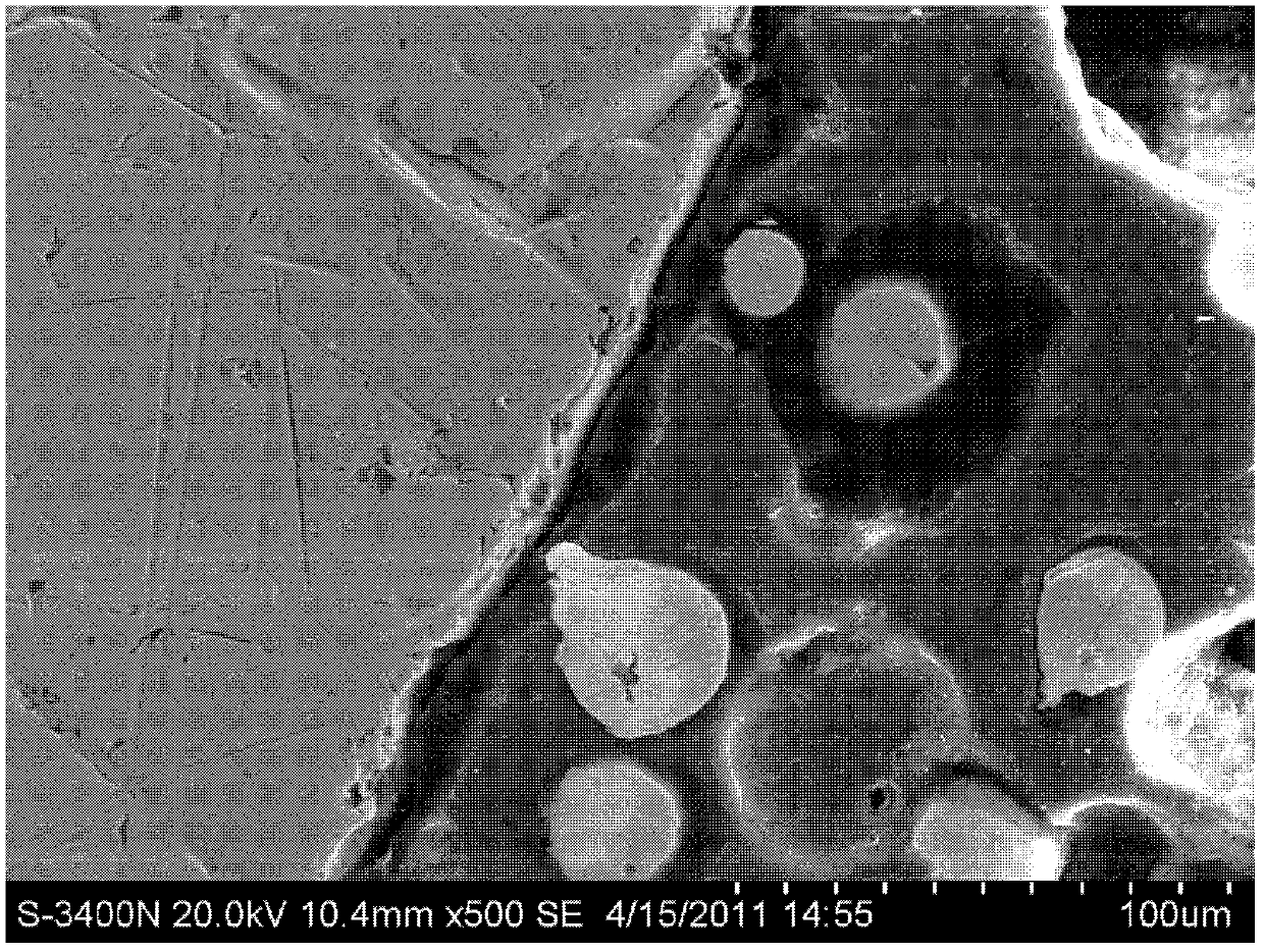
[0039] In order to make the plastic conductive, the present invention uses raw materials: epoxy resin as the substrate, ethylenediamine as the curing agent, silver-coated copper powder as the conductive particles (metal silver 18%, metal copper 82%; particle size is 30%). ~50μm). Required experimental equipment: glass rod, medicine spoon, polishing liquid, polishing cloth, plastic cup, 5 cylindrical molds, and 5 copper pieces of internal organization to be observed, electronic balance. Specific methods include the following:

[0040] 1. Weigh 80 g of epoxy resin, 8 g of ethylenediamine, and 160 g of silver-coated copper powder with an electronic balance in proportion and place them in three identical plastic cups.

[0041] 2. Add ethylenediamine to the plastic cup filled with epoxy resin and stir evenly.

[0042] 3. Slowly add silver-coated copper powder, stirring while adding it, to prevent too fast curing to form agglomerates, resulting in uneven dispersion of the remaining silve...

Embodiment 2

[0050] In order to reduce the cost and make the experiment more economical, the present invention can also replace the expensive silver-coated copper powder with relatively inexpensive tin-silver copper powder. Experimental raw materials: base material epoxy resin, curing agent ethylenediamine, conductive particles tin silver copper powder (metal silver 3%, metal copper 0.5%, 96.5% metal tin; particle size is 30-50μm in diameter), required experiment Utensils: glass rods, medicine spoons, polishing liquid, polishing cloth, plastic cups, 5 cylindrical molds, and 5 copper plates for observation of internal tissues, electronic balance. Specific methods include the following:

[0051] 1. Use an electronic balance to weigh out 80g of epoxy resin, 8g of ethylenediamine, and 160g of tin, silver and copper powder, and place them in three different plastic cups.

[0052] 2. Add ethylenediamine to the plastic cup filled with epoxy resin and stir evenly.

[0053] 3. Slowly add tin-silver-copp...


PUM

PropertyMeasurementUnit
diameteraaaaaaaaaa
electrical resistivityaaaaaaaaaa

Abstract

The invention discloses conducting resin for a scanning electronic microscope and a preparation method thereof, which belongs to the technical field of resin composite materials. The conducting resin adopts epoxy resin as a base material, ethylene diamine as a curing agent, and tin-silver-copper powder or silver-coated copper powder as conductive particles, and comprises the following components by mass percent: 32-34% of epoxy resin, 3-4% of ethylene diamine and 62-65% of tin-silver-copper powder or silver-coated copper powder. Ethylene diamine is added into epoxy resin and simultaneously uniformly stirred; the conductive particles are added and stirred at the same time till the conductive particles are completely uniformly dispersed and glue-like mixture reaches a substantially cured degree; the glue-like mixture is added into a die; and the glue-like mixture is dried and cured at room temperature, and then samples are taken out. The conducting resin can fully meet the requirements of SEM (scanning electron microscope) observation.

Description

Technical field [0001] The invention uses material processing technology in materials science and engineering for the observation of metal samples by a scanning electron microscope, and belongs to the technical field of resin composite materials. Background technique [0002] An optical microscope is an optical instrument that uses optical principles to magnify and image tiny objects that cannot be distinguished by the human eye, so that people can extract detailed structure information. Scanning electron microscope (abbreviated as "scanning electron microscope" or "SEM") is a microscopic observation method between transmission electron microscope and optical microscope, which can directly use the material properties of the sample surface material for microscopic imaging. [0003] In principle, the scanning electron microscope uses a focused, very thin, high-energy electron beam to scan on the sample to excite various physical information. Through the acceptance, magnification and...

Claims


Application Information

Patent Timeline
Patent Type & Authority Patents(China)
IPC IPC(8): C08L63/00C08K13/02C08K5/17C08K3/08C09D163/00C09D5/00C09D5/16
Inventor 郭福马立民徐广臣吴丹殷晓飞阎海亮章亚建肖庆丰
Owner BEIJING UNIV OF TECH
Learn More