Method for restraining secondary emission of surface nano-structure of microwave component

A technology of secondary electron emission and nanostructure, which is applied in the direction of microstructure technology, microstructure device, manufacturing microstructure device, etc. The effect of raising the discharge threshold

Inactive Publication Date: 2012-06-27
XI AN JIAOTONG UNIV +1
View PDF4 Cites 20 Cited by
  • Summary
  • Abstract
  • Description
  • Claims
  • Application Information

AI Technical Summary

Problems solved by technology

The first way is to prepare new low-SEY coating materials on the surface of components, such as Alodine, TiN, AgO, etc. The significant advantages of these coatings are small surface SEY and good environmental stability, but this method has disadvantages, that is, the coating itself is conductive Poor performance leads to large surface impedance under high frequency conditions, which is difficult to popularize in engineering
The second way is to form a large roughness on the surface of the silver coating, and use the principle that the secondary electrons are reflected and absorbed in the structure gap with large roughness to reduce the average SEY of the surface, thereby increasing the micro-discharge threshold of microwave components. The advantages of this method are: ...

Method used


Image

  • Method for restraining secondary emission of surface nano-structure of microwave component
  • Method for restraining secondary emission of surface nano-structure of microwave component
  • Method for restraining secondary emission of surface nano-structure of microwave component

Examples


Embodiment Construction

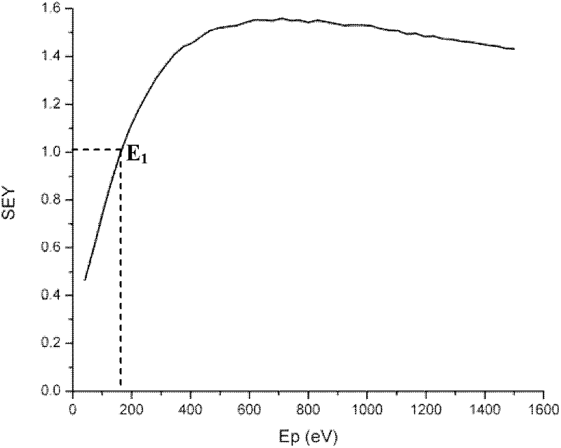
[0027] like figure 1 As shown, the SEY test curve of the electrochemical silver-plated surface on a typical aluminum alloy substrate, the abscissa is the initial energy of the electron incident on the metal surface, when the free electrons in the cavity meet Ep>E under the condition of microwave field acceleration 1 When (E 1 The incident is the electron energy point), and micro-discharge may occur.

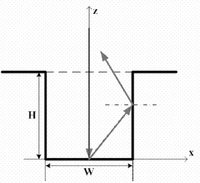
[0028] On the basis of obtaining the SEY curve of the surface of the actual microwave component on the satellite, the scale of the nanostructure is limited to below 100nm, which is far smaller than the rough undulation scale of the mechanical processing of the microwave cavity and the subsequent electrochemical surface coating. Therefore, the surface of the actual microwave component is viewed as is an approximately smooth surface.

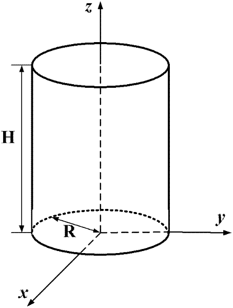
[0029] The Monte-Carlo method (M-C method) is used to simulate the collision, absorption, and collision, absorption, and escape of electrons incid...


PUM


Abstract

A method for restraining the secondary emission of a surface nano-structure of a microwave component comprises the following steps that: a metal nano-structure is formed on a good conductor layer of a microwave component basal body; different test conditions are selected, and comprise the porosity, depth-to-width ratio and shape of the nano-structure; a Monte-Carlo simulation is utilized to simulate the collision and absorption processes of an electron which enters the nano-structure and the collision, absorption and escape processes of a secondary electron which is produced by the electron, and the secondary emission yield of a single nano-structure is theoretically obtained; and according to the principle of secondary emission yield, various surface treatment technologies are utilized to adjust the shape, depth-to-width ratio and porosity of the surface nano-structure of the microwave component, so the secondary emission yield is the minmum. The method can greatly improve the micro discharge threshold of the microwave component which undergoes the electrochemical silvering surface treatment; and the secondary electron trap structure with high depth-to-width ratio is easier to realize, the influence on surface roughness can be neglected to a certain extent, and negative effects which are caused by restraining the secondary emission yield (SEY) of the current large roughness structure surface are solved.

Description

Technical field: [0001] The patent of the present invention relates to the field of surface treatment of microwave components, in particular to a method for suppressing secondary electron emission by nanostructures on the surface of microwave components. Background technique: [0002] At present, most of the microwave passive components in the satellite payload system are based on aluminum alloy. In order to reduce the loss of the device, the most commonly used method is the surface electrochemical silver plating. In actual use, these silver-plated parts are prone to multiplier discharge effect under the condition of high-power electromagnetic wave transmission, which is called micro-discharge phenomenon. Micro-discharge breakdown of microwave components is one of the main factors that determine the reliability and life of satellites. One of the necessary conditions for the occurrence of micro-discharge is that the average secondary electron emission coefficient on the cavi...

Claims


Application Information

Patent Timeline
IPC IPC(8): B81C1/00
Inventor 贺永宁叶鸣崔万照王瑞胡天存黄光孙
Owner XI AN JIAOTONG UNIV
Why Eureka
Try Eureka