

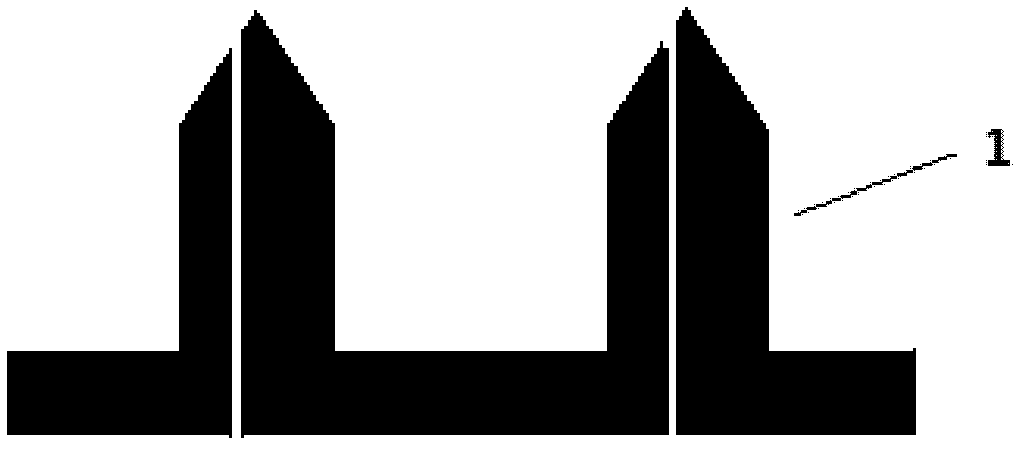
Anomalous plane hollow microneedle based on surface micro processing process and preparation method thereof
A microfabrication and hollow microtechnology, which is applied in the direction of microneedles, needles, medical devices, etc., can solve the problems of complex and cumbersome steps, unfavorable mass production, and height restrictions of microneedles, and achieve simple and easy process and rapid replication And the effect of high-speed mass production, wet etching and simple operation of casting
- Summary
- Abstract
- Description
- Claims
- Application Information
AI Technical Summary
Problems solved by technology
Method used
Image

Examples
Embodiment 1
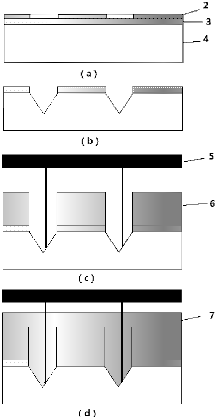
[0025] Such as figure 2 As shown, this embodiment includes the following steps:
[0026] Step 1: Prepare a p-type boron-doped polished wafer 4 with crystal orientation as a substrate. A layer of positive resist 2 with a thickness of 5 μm is thrown on it, and developed by photolithography, and the mask plate has a square pattern.
[0027] The second step: using HF wet etching process to remove the silicon oxide 3 at the part not covered by the positive resist.
[0028] Step 3: Etching the silicon wafer treated in the second step with KOH with a mass fraction of 30% to obtain an inverted quadrangular pyramid structure.
[0029] Step 4: Throw a layer of SU-8 glue 6 with a thickness of 300 μm, and develop it by photolithography. The mask plate has a circular structure.
[0030] Step 5: Load the molybdenum wire array plate 5 into the obtained concave mold. The molybdenum wire array is obtained by performing photolithography, development and electroplating on the photoresist, a...
Embodiment 2
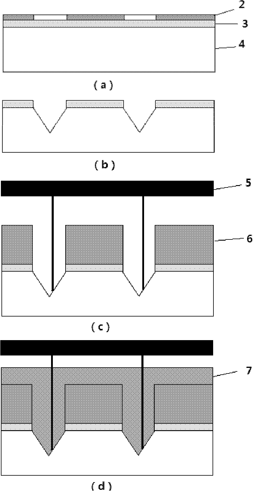
[0034] Such as figure 2 As shown, this embodiment includes the following steps:
[0035] Step 1: Prepare a p-type boron-doped polished wafer 4 with crystal orientation as a substrate. A layer of positive resist 2 with a thickness of 5 μm is thrown on it, and developed by photolithography, and the mask plate has a square pattern.
[0036] The second step: using HF wet etching process to remove the silicon oxide 3 at the part not covered by the positive resist.
[0037] Step 3: Etching the silicon wafer treated in the second step with KOH with a mass fraction of 30% to obtain an inverted quadrangular pyramid structure.
[0038] Step 4: Throw a layer of SU-8 glue 6 with a thickness of 200 μm, and develop it by photolithography. The mask plate has a circular structure.
[0039] Step 5: Load the molybdenum wire array plate 5 into the obtained concave mold. The molybdenum wire array is obtained by performing photolithography, development and electroplating on the photoresist, a...
PUM
| Property | Measurement | Unit |
|---|---|---|
| Radius | aaaaa | aaaaa |
| Length | aaaaa | aaaaa |
Abstract
Description
Claims
Application Information