Array type continuously-flowing microfluidic chip device and manufacture method and application thereof

A microfluidic chip, microchip technology, applied in chemical instruments and methods, chemical/physical/physical chemical processes, chemical/physical processes, etc., can solve complex and expensive external equipment reaction reagents, unable to deliver fresh reaction solution in time, etc. problem, to achieve the effect of low cost

Active Publication Date: 2012-07-04
INST OF CHEM CHINESE ACAD OF SCI
View PDF5 Cites 24 Cited by
  • Summary
  • Abstract
  • Description
  • Claims
  • Application Information

AI Technical Summary

Problems solved by technology

[0006] The solid-phase synthesis technology based on the microchip platform is currently also reported (Science, 2007, 318, 1888-1888., Proteomics, 2003, 3, 2135-2141., invention patent: combined compound array chip and preparation method, 03112772. X), but these solid-phase synthesis is often a static reaction, cannot transport fresh reaction solution in time, and requires complex and expensive external equipment and special reaction reagents

Method used


Image

  • Array type continuously-flowing microfluidic chip device and manufacture method and application thereof
  • Array type continuously-flowing microfluidic chip device and manufacture method and application thereof
  • Array type continuously-flowing microfluidic chip device and manufacture method and application thereof

Examples


Embodiment 1

[0047] Example 1. Fabrication of array type continuous flow microfluidic chip device

[0048] (1) Fabrication of six-channel synthesis reaction microchip

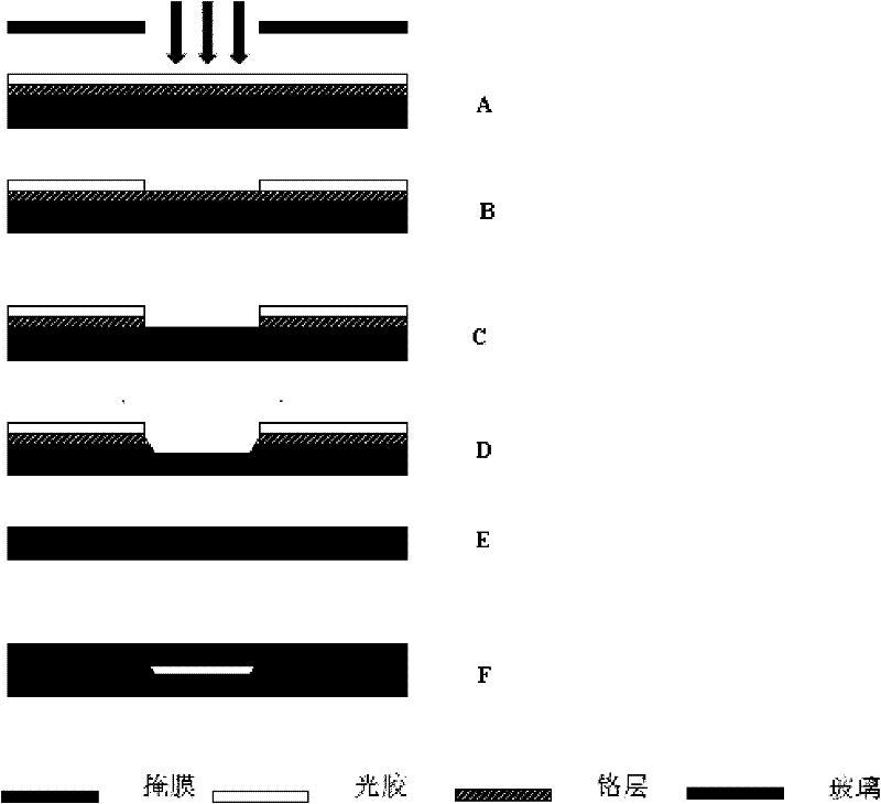
[0049] The manufacturing process of the six-channel synthesis reaction microchip is as follows image 3 As shown, step A represents an exposure step, step B represents a development step, step C represents a chromium removal step, step D represents an etching step, step E represents a photoresist and chromium removal step, and step F represents a bonding step.

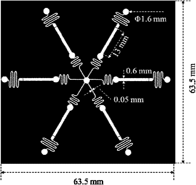
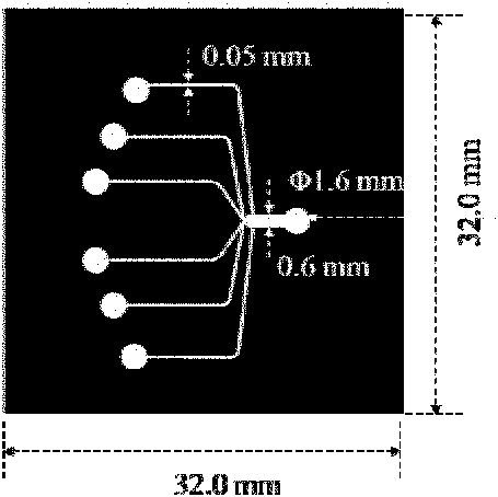
[0050] The microchannel size design of the synthetic reaction microchip is as follows figure 1 As shown, the designed synthetic reaction microchip pattern is made into a film mask by laser phototypesetting; the film mask is covered on a 63.5mm×63.5mm×1.5mm homogenous chrome plate (chrome type: LRC; chrome thickness: 145nm; glue thickness: 570nm), exposed to UV light (365nm) for 8 seconds; the exposed chromium plate is developed in a 0.7% NaOH aqueous solution by mass, and ...

Embodiment 2

[0061] Example 2. Using the continuous flow microfluidic chip device made in Example 1 to perform the peptide synthesis reaction of each reaction unit

[0062] (1) Preparation of solid phase carrier

[0063] The carrier resin used in solid-phase peptide synthesis in conventional containers has a relatively low degree of cross-linking and swells in an organic solvent atmosphere. If the swollen resin is filled into the reaction chamber of the microfluidic chip, it will deform and block the microchannel. Therefore, the highly cross-linked rigid carrier microspheres suitable for the microfluidic chip device of the present invention are prepared by the seed one-step swelling polymerization method, and the specific preparation method is as follows:

[0064] a. Preparation of polyethylene (PS) seeds: According to literature (Macromolecules, 1990, 23, 3104-3109.), PS seeds with a particle size of about 10 μm were prepared.

[0065] b. The oil phase of the reaction system includes 2.5 mL of 4...

Embodiment 3

[0085] Example 3. The Fmoc-Leu, Fomc-Ser and Fmoc-Phe modified solid-phase peptide synthesis carriers prepared in Example 2 were used as solid-phase carriers, and the continuous flow microfluidic chip device made in Example 1 was used for integrated solidification. Phase peptide synthesis reaction

[0086] (1) According to the method reported in the literature (Combinatorial Chemistry, Oxford University Press, 1998, ch. 3, pp. 42-43.), six kinds of anti-β-endorphin 3E7 mAb affinity peptide library with higher affinity activity were synthesized Polypeptides YGAFLS (AR1), YGAFS (AR2), YGAFL (AR3), YGGFLS (AR4), YGAF (AR5) and YGALS (AR6).

[0087] The specific synthesis steps are as follows:

[0088] a. Use a precision syringe pump to push a 1mL syringe through the sub-injection port 3 to inject the hydroxymethyl phenol methyl polystyrene resin microspheres prepared in Example 2 dispersed in DMF into the reaction chamber 4 respectively. The cavity 4 is filled with six resins prepared...


PUM


Abstract

The invention provides an array type continuously-flowing microfluidic chip device and a manufacture method and application thereof. The device comprises a synthetic reaction microchip, a flow splitting microchip and a reagent charge cell, wherein reaction cavity bodies of various reaction units in the synthetic reaction microchip are internally provided with multiple layers of fences and barrages with cofferdam type structures, so that a solid-phase synthesis carrier can be effectively bounded, and the continuous fluid is also guaranteed to be smooth; and a charge module is composed of the flow splitting microchip and the reagent charge cell, so that independent and simultaneously sample introduction of different reagents can be conducted into various reaction units of the synthesis microchip. The microfluidic chip device provided by the invention can be used for the multi-step solid-phase synthesis reaction, the efficiency is high, the amount of reagents used is few, and the manufacture cost is low.

Description

Technical field [0001] The invention relates to an array type continuous flow microfluidic chip device and a manufacturing method and application thereof, belonging to the technical field of microreactors. Background technique [0002] Lab on a chip has developed into one of the most cutting-edge scientific and technological fields in the world today (Sens. Actutors, B, 1990, 1, 244-248.). It uses microfluidic chips as its core technology. Chemistry, biology, medicine and other fields have very attractive development prospects. Microfluidic chip technology integrates or basically integrates basic operation units such as pre-processing, sample addition, reaction, separation, analysis, cell culture, etc., involved in the fields of chemistry and biology on a square-inch chip to replace conventional chemistry. Or a technology platform for various functions of biological laboratories. The microfluidic chip has the characteristics of large specific surface area, fast mass and heat tr...

Claims


Application Information

Patent Timeline
Patent Type & Authority Applications(China)
IPC IPC(8): B01J19/00
Inventor 赵睿王蔚芝黄嫣嫣刘吉众刘国诠
Owner INST OF CHEM CHINESE ACAD OF SCI
Why Eureka
Try Eureka