Preparation method for transmission electron microscope (TEM) specimen of cadmium zinc tellurium (CdZnTe) and metal interface

An electron microscope and metal interface technology, applied in the preparation of test samples, etc., can solve the problems of sample fragmentation and high rejection rate, and achieve the effect of preventing sample fragmentation, improving the success rate and reducing damage.

Inactive Publication Date: 2012-07-04
NORTHWESTERN POLYTECHNICAL UNIV
View PDF5 Cites 15 Cited by
  • Summary
  • Abstract
  • Description
  • Claims
  • Application Information

AI Technical Summary

Problems solved by technology

[0006] In order to overcome the shortcomings of the existing preparation method in the preparation of CdZnTe and metal interface TEM samples that are prone to sample fragmentation and lead to high scrap rate, the present invention provides a transmission electron microscope sample preparation method for CdZnTe and metal interface

Method used


Image

  • Preparation method for transmission electron microscope (TEM) specimen of cadmium zinc tellurium (CdZnTe) and metal interface
  • Preparation method for transmission electron microscope (TEM) specimen of cadmium zinc tellurium (CdZnTe) and metal interface
  • Preparation method for transmission electron microscope (TEM) specimen of cadmium zinc tellurium (CdZnTe) and metal interface

Examples


Embodiment 1

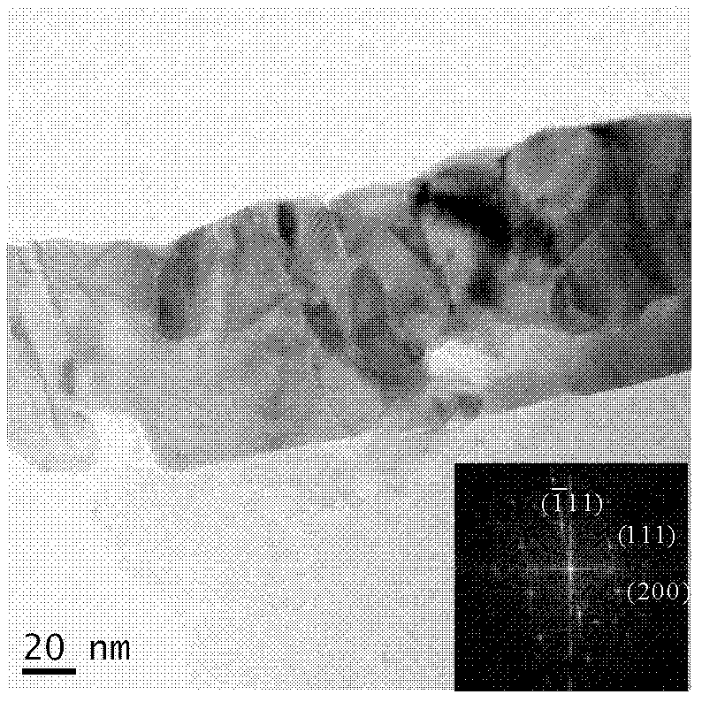
[0018] Embodiment 1: In the first step, the CdZnTe crystal is wire-cut, and the cut wafers have a size of 3mm×5mm×0.7mm, a total of 3 pieces, and the wafers are cleaned and mechanically polished to obtain 3 CdZnTe wafers to be used.

[0019] The second step is to prepare Au electrodes in the ZHD-300 resistance evaporation coating machine. One of the samples is a double-sided coated electrode, and the rest of the samples are single-sided coated with an electrode thickness of 100nm. at 200°C for 5 minutes.

[0020] In the third step, the three wafers are bonded in such a way that the Au electrode layers are facing each other. The adhesive is Gatan G-1 glue, and the mixing ratio of soft and hard glue is 10:1. Bake on hot plate for 15 hours.

[0021] The fourth step is to use 2000# sandpaper to manually thin the sample to 100 μm. The thinning direction is along the normal direction of the bonding gap. network.

[0022] In the fifth step, use a manual grinder and 5000# sandpaper...

Embodiment 2

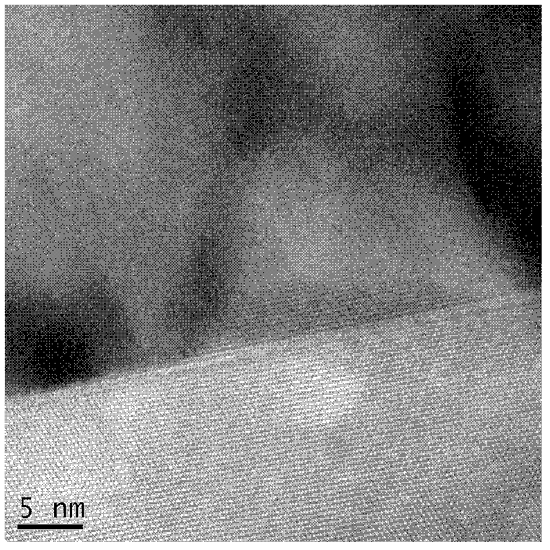
[0024] Embodiment 2: the first step, wire cutting is carried out to CdZnTe crystal, the wafer size that cuts out is 3mm * 5mm * 0.7mm, totally 5 pieces, wafer is cleaned, mechanically polished, in 2%Br-MeOH, wafer is carried out Corrosion to obtain 5 CdZnTe wafers to be used.

[0025] The second step is to prepare Au electrodes in the ZHD-300 resistance evaporation coating machine. One of the samples is a double-sided coated electrode, and the rest of the samples are single-sided coated with an electrode thickness of 100nm. at 200°C for 5 minutes.

[0026] In the third step, the three wafers are bonded in such a way that the Au electrode layers are facing each other. The adhesive is Gatan G-1 glue, and the mixing ratio of soft and hard glue is 10:1. Bake on hot plate for 20 hours.

[0027] The fourth step is to manually thin the sample to 100 μm with 3000# sandpaper, and the thinning direction is along the normal direction of the bonding gap. network.

[0028] In the fifth...

Embodiment 3

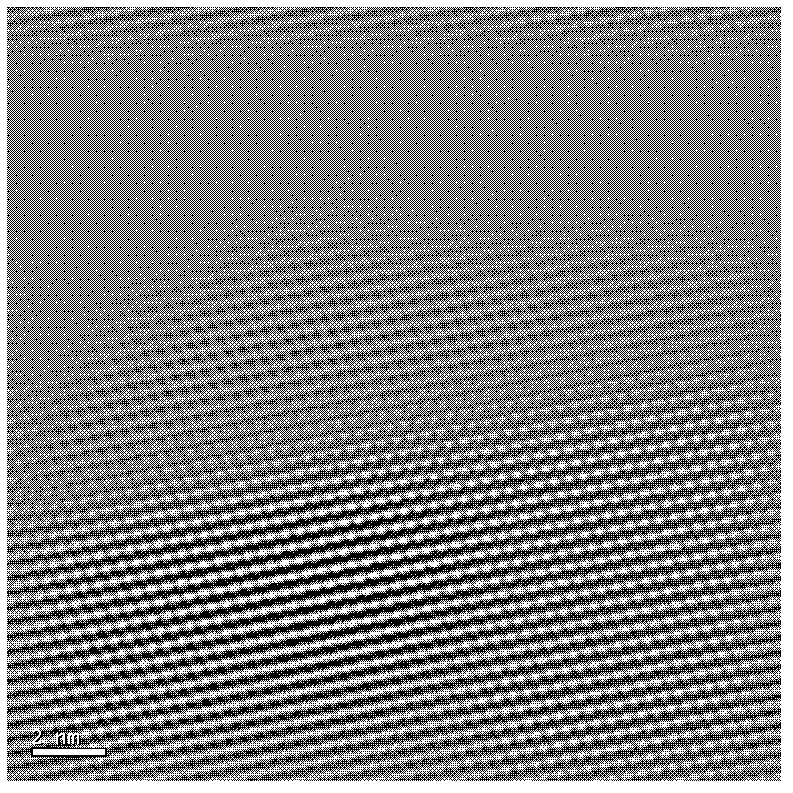
[0030] Embodiment 3: the first step, carry out wire cutting to CdZnTe crystal, the wafer size that cuts out is 3mm * 5mm * 0.7mm, totally 5 pieces, the wafer is cleaned, mechanically polished, in 2% Br-MeOH, wafer is carried out Corrosion to obtain 5 CdZnTe wafers to be used.

[0031] The second step is to prepare Al electrodes in a ZHD-300 resistance evaporation coating machine. One of the samples is a double-sided coated electrode, and the rest of the samples are single-sided coated with an electrode thickness of 100nm, and then undergo rapid annealing under a nitrogen atmosphere. at 200°C for 5 minutes.

[0032] In the third step, the three wafers are bonded in such a way that the Al electrode layers are facing each other. The adhesive is Gatan G-1 glue, and the mixing ratio of soft and hard glue is 10:1. After the bonding is completed, the sample is tightened with a clamp. Bake on hot plate for 20 hours.

[0033] The fourth step is to manually thin the sample to 100 μm w...


PUM

PropertyMeasurementUnit
thicknessaaaaaaaaaa

Abstract

The invention discloses a preparation method for a transmission electron microscope (TEM) specimen of a cadmium zinc tellurium (CdZnTe) and metal interface. The preparation method is used for solving the technical problem that the reject rate is high because the specimen is broken very easily when the TEM specimen of the CdZnTe and metal interface is prepared in the prior art. The technical scheme is that the preparation method comprises the following steps of: after a CdZnTe single crystal is linearly cut, washed and polished, conducting chemical corrosion; preparing a metal electrode in a resistive evaporation coating machine; folding and sticking the specimen and drying the specimen on a heating table; and grinding, polishing and thinning the specimen along the normal line direction ofa sticking gap, polishing the two surfaces of the specimen, sticking a copper grid on one surface, using a manual grinder to thin the specimen, and finally using a Gatan 691 ion mill to thin the specimen till the specimen is punctured. Since a multi-piece sticking method and a manual grinder for grinding and polishing through high-grade abrasive paper are adopted, after thinning and polishing arecompleted, the damage caused to an interface area in the thinning process is minimized and the success rate of specimen preparation is improved. The success rate of specimen preparation is improved from 30-40 percent in the background technology to 60-70 percent.

Description

technical field [0001] The invention relates to a method for preparing a transmission electron microscope sample, in particular to a method for preparing a transmission electron microscope sample at the interface between cadmium zinc telluride and a metal. Background technique [0002] As an important material for preparing X-ray and γ-ray detectors, CdZnTe's contact performance with surface metal electrodes has an important impact on the performance of CdZnTe detectors. And if the structural state of the contact interface can be determined, it will undoubtedly have great theoretical guiding significance for improving the performance of CdZnTe detectors. At present, there are no relevant reports on the preparation of transmission electron microscopy samples at the interface between CdZnTe materials and metals, and there are only reports on the preparation of transmission electron microscopy samples at the interface between other semiconductor materials or metal-semiconductor...

Claims


Application Information

Patent Timeline
Patent Type & Authority Applications(China)
IPC IPC(8): G01N1/28G01N1/32
Inventor 傅莉孙颉聂中明
Owner NORTHWESTERN POLYTECHNICAL UNIV
Why Eureka
Try Eureka