

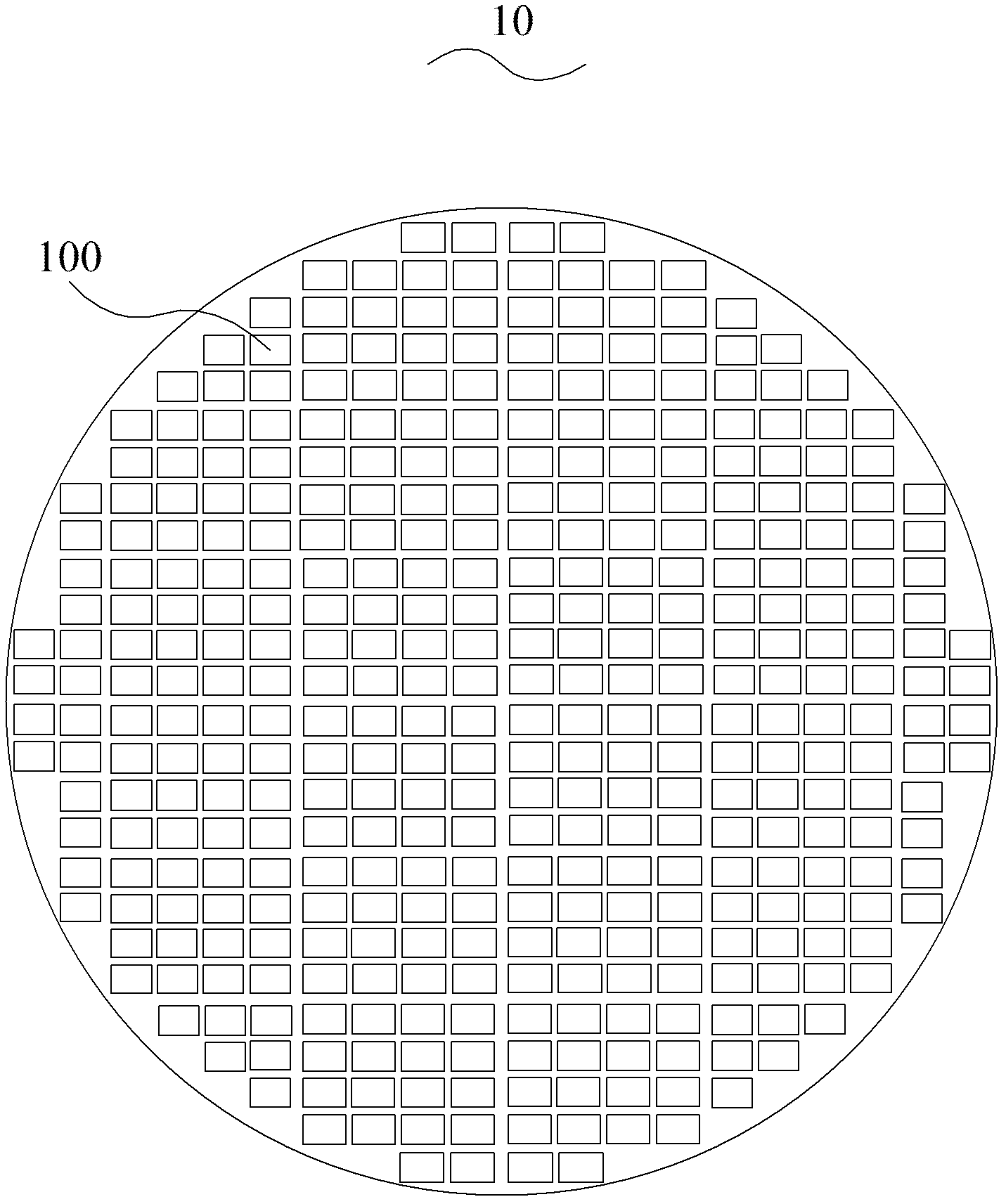
Cylindrical bump packaging structure
A packaging structure and column bump technology, applied in electrical components, electric solid devices, circuits, etc., can solve the problems of short circuit of solder bumps, easy dripping between solders, affecting welding quality, etc., to prevent short circuits and improve reliability. , The effect of saving material cost
- Summary
- Abstract
- Description
- Claims
- Application Information
AI Technical Summary
Problems solved by technology
Method used
Image

Examples
Embodiment Construction
[0032] The specific embodiments of the present invention will be described in detail below in conjunction with the accompanying drawings.
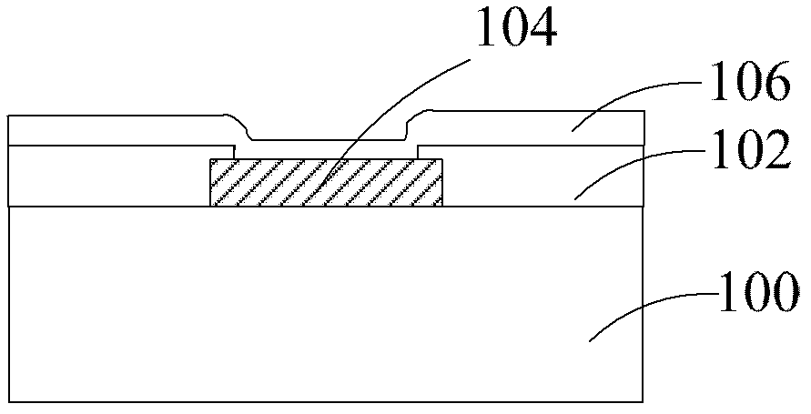
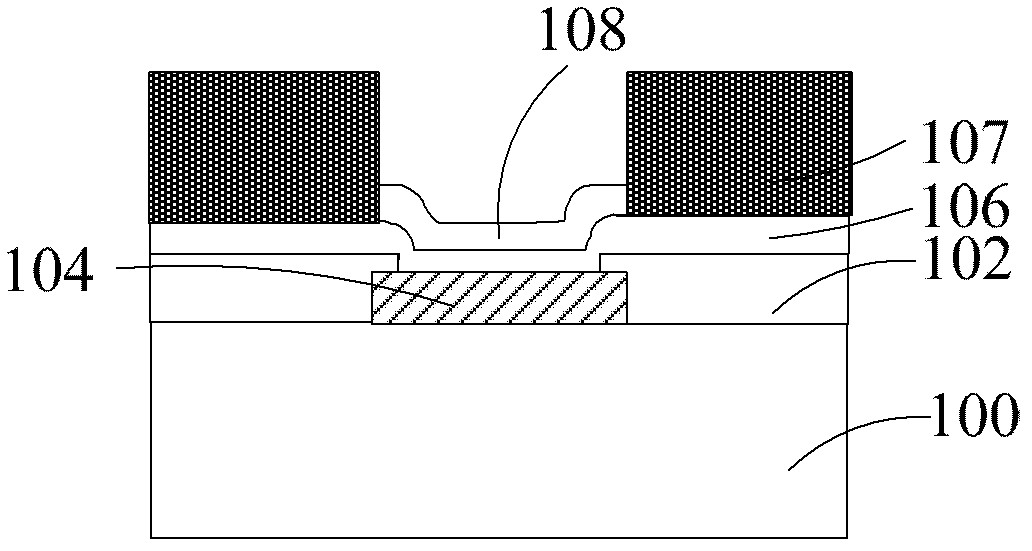
[0033] figure 2 It is a schematic diagram of a stud bump package structure according to the present invention, and the package structure includes: a chip 300 , an UBM layer 303 , a copper column 305 , an oxide layer 307 and a solder bump 306 .
[0034] The upper surface of the chip 300 is provided with a pad 301 and a passivation layer 302 , and the passivation layer 302 covers the upper surface of the chip 300 except for the opening of the pad 301 .
[0035] An UBM layer 303 is disposed on the pad 301 , and the UBM layer 303 includes a heat-resistant metal layer and a metal-wetting layer sequentially from bottom to top. Specifically, the material of the heat-resistant metal layer is titanium, chromium, tantalum or a combination thereof; the material of the metal wetting layer is copper, aluminum, nickel or a combination thereof.
[003...
PUM
| Property | Measurement | Unit |
|---|---|---|
| Thickness | aaaaa | aaaaa |
| Thickness | aaaaa | aaaaa |
| Thickness | aaaaa | aaaaa |
Abstract
Description
Claims
Application Information