Eureka AIR delivers breakthrough ideas for toughest innovation challenges, trusted by R&D personnel around the world.

Insulated gate bipolar translator (IGBT) device with two short-circuit positive electrodes

A double-anode, short-circuit technology, applied in semiconductor devices, electrical components, circuits, etc., can solve the problems of increased IGBT turn-off loss, increased turn-off time, slow extraction speed, etc., to reduce turn-off time and improve temperature characteristics. , the effect of increasing the injection efficiency

Inactive Publication Date: 2012-07-04
UNIV OF ELECTRONICS SCI & TECH OF CHINA +1
View PDF3 Cites 7 Cited by
  • Summary
  • Abstract
  • Description
  • Claims
  • Application Information

AI Technical Summary

Problems solved by technology

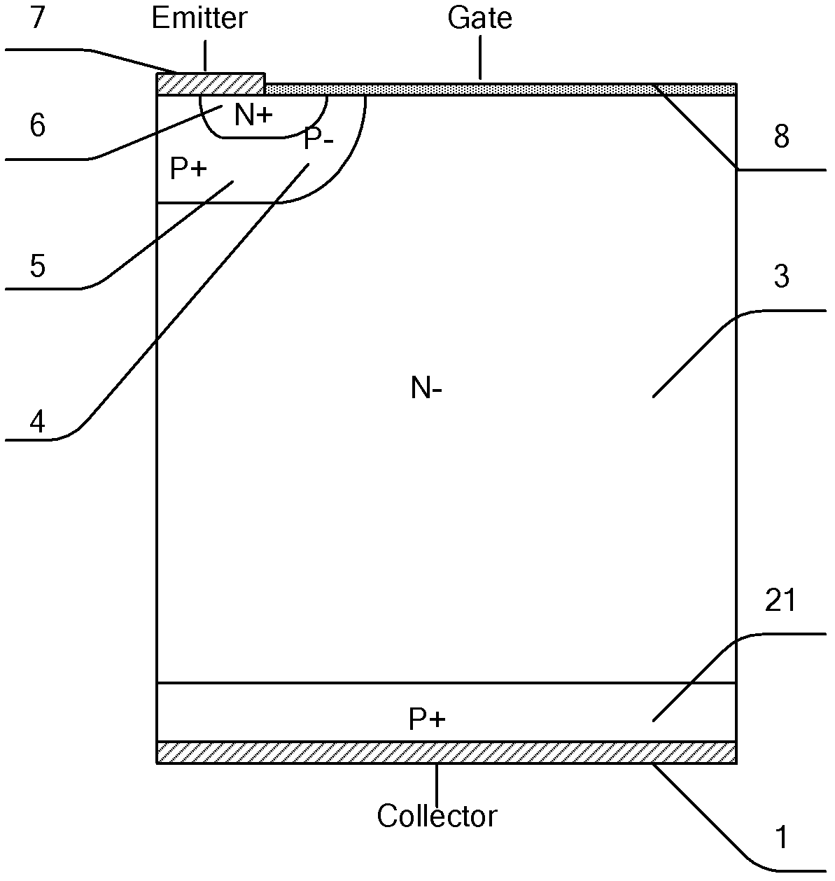
However, the SA-NPN structure extracts electrons through the NPN transistor when it is turned off. The extraction speed is slower than that of the anode short-circuit structure and has a certain tail current, which increases the turn-off time, which will lead to an increase in the turn-off loss of the IGBT.

Method used


Image

  • Insulated gate bipolar translator (IGBT) device with two short-circuit positive electrodes
  • Insulated gate bipolar translator (IGBT) device with two short-circuit positive electrodes
  • Insulated gate bipolar translator (IGBT) device with two short-circuit positive electrodes

Examples


Embodiment Construction

[0029] By adopting the dual-anode short-circuit planar insulated gate bipolar transistor of the present invention, the contradictory relationship between the turn-on voltage drop and the turn-off loss of the insulated gate bipolar transistor can be better compromised. With the development of semiconductor technology, more high withstand voltage devices can be produced by adopting the invention.

[0030] 1. Plannar NPT type IGBT device with double anode short circuit

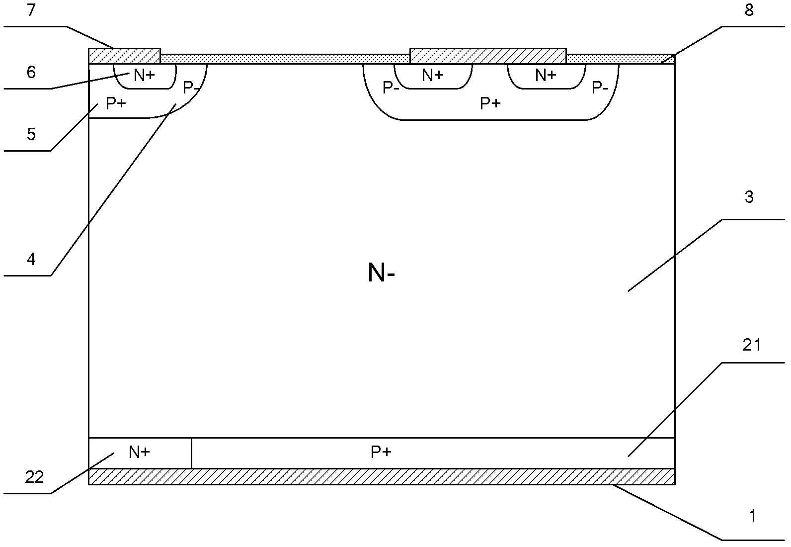
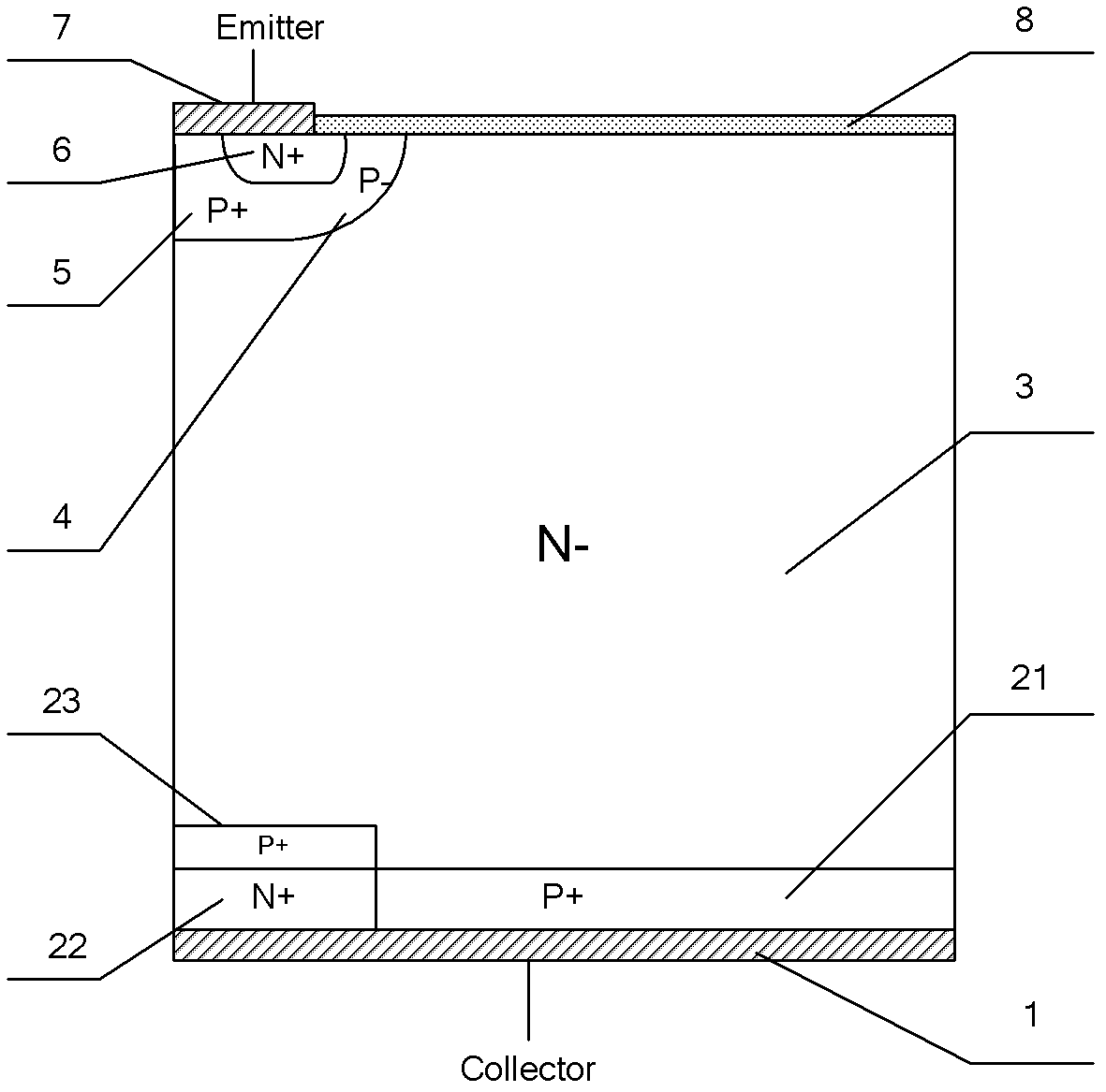
[0031] like Figure 4 As shown, the device includes an anode structure, a drift region structure and a cathode structure. The anode structure is a double anode short-circuit structure, including a first P+ hole emission layer 21, a second P+ hole emission layer 23, a metal collector 1 and a silicon dioxide barrier layer 10; the silicon dioxide barrier layer 10 Located on the back side of the first P+ hole emission layer 21; the metal collector 1 is located on the side of the first P+ hole emission layer 21 and ...


PUM


Abstract

The invention discloses an insulated gate bipolar translator (IGBT) device with two short-circuit positive electrodes, and belongs to the technical field of semiconductor power devices. A positive electrode structure of the device is a two-positive-electrode short-circuit structure. The IGBT device comprises a first P+ hole emission layer, a second P+ hole emission layer, a metal collector and a silicon dioxide barrier layer, wherein the silicon dioxide barrier layer is positioned on the back face of the first P+ hole emission layer; the metal collector is positioned on the side face of the first P+ hole emission layer and below the second P+ hole emission layer, and the two P+ hole emission layers are contacted with each other; the second P+ hole emission layer is positioned at the bottom of an N- drift region and staggered in parallel with the first P+ hole emission layer; and an electronic trench is formed between the first P+ hole emission layer and the second P+ hole emission layer. The positive electrode structure of the IGBT device is improved, so that the hole injection efficiency is improved, the current carrier concentration distribution in the drift region is optimized, the conductivity modulation performance in the device body is improved, a negative differential resistance (NDR) region is eliminated effectively, the cut-off loss of the IGBT device is reduced effectively, and finally, compromise optimization for conductivity pressure drop and cut-off loss is realized.

Description

technical field [0001] The invention belongs to the technical field of semiconductor power devices, and relates to an insulated gate bipolar transistor (IGBT). Background technique [0002] In recent years, with the rapid development of microelectronics technology, society has continuously increased the requirements for the most advantageous power devices in electronic power, and the advantages of insulated gate bipolar transistors, one of the representatives of power devices, have attracted widespread attention. Insulated gate bipolar transistors (IGBTs) are composed of bipolar transistors and power metal-oxide-semiconductor field-effect transistors. Due to their characteristics of voltage control, reduced conduction voltage, high input impedance, simple drive circuit, and wide safe operating area, It is widely used in air conditioners, inverters, induction cookers, etc., as well as fields requiring fast and low loss. [0003] Traditional non-punch-through (NPT) IGBT (stru...

Claims


Application Information

Patent Timeline
Patent Type & Authority Applications(China)
IPC IPC(8): H01L29/739H01L29/417
Inventor 李泽宏陈伟中安俊杰张波
Owner UNIV OF ELECTRONICS SCI & TECH OF CHINA
Why Eureka
Eureka Blog
Learn More