Method for efficiently packaging light-emitting diode (LED) chips by using substrate high diffuse reflection optical design

A technology for LED chips and LED packaging, applied in electrical components, circuits, semiconductor devices, etc., can solve problems such as reducing the reflectivity of the blue light band, reducing the luminous efficiency and color rendering index of the packaged LED, and affecting the efficiency of the LED light source.

Active Publication Date: 2012-07-04
FUJIAN INST OF RES ON THE STRUCTURE OF MATTER CHINESE ACAD OF SCI
View PDF3 Cites 11 Cited by
  • Summary
  • Abstract
  • Description
  • Claims
  • Application Information

AI Technical Summary

Problems solved by technology

However, this high-reflection film system will cause the reflected light to be concentrated, and more than 80% of the light is concentrated in a relatively narrow reflection area light column, such as figure 1 The dotted line F-G-H-I in the fan-shaped area has an angle of 60°, which leads to significant glare, especially for transparent sealants mixed with phosphor powder, the small laser surface will cause the area

Method used


Image

  • Method for efficiently packaging light-emitting diode (LED) chips by using substrate high diffuse reflection optical design
  • Method for efficiently packaging light-emitting diode (LED) chips by using substrate high diffuse reflection optical design
  • Method for efficiently packaging light-emitting diode (LED) chips by using substrate high diffuse reflection optical design

Examples


Embodiment 1

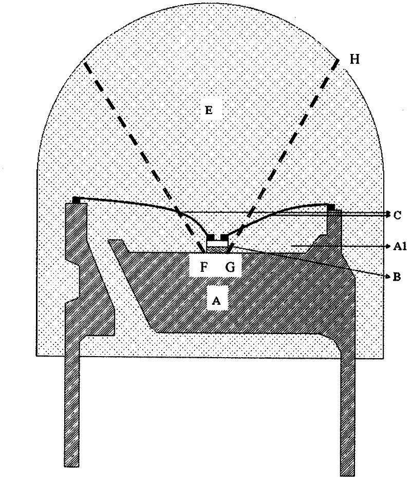
[0022] refer to figure 2 and image 3 , the present invention is implemented like this:

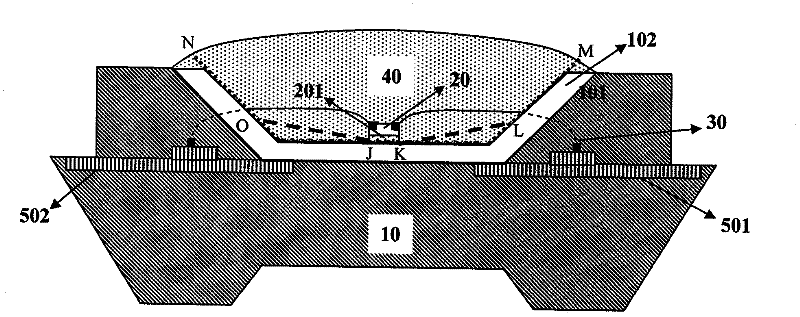
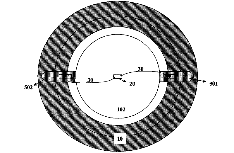
[0023] On the upper surface 101 of the LED packaging substrate 10 made of aluminum or copper or iron or ceramics or circuit boards, the surface diffuse reflection layer 102 is processed to make it have a diffuse reflectance greater than 80%, a specular reflection and a transmittance lower than 20% of the surface. The upper surface layer 102 with high diffuse reflection can be made of ceramic film with high diffuse reflection, ceramic glaze, inorganic or organic coating, Teflon film, etc., or even the surface of high white ceramic body. In Example 1, an ultra-white glaze with a diffuse reflection of 98% in the wavelength range of 200nm-760nm (that is, a whiteness of 98 at the same time) is used to coat the Cu substrate to form the high diffuse reflection layer 102 .

[0024] Install the pre-designed electrodes 501 and 502 on the corresponding positions of the substrate 10 and fix them ...

Embodiment 2

[0030] Embodiment 2 of the present invention is similar to the above embodiment column 1, but the high diffuse reflection glaze layer 102 of the above embodiment 1 is replaced by a barium sulfate coating or an aluminum oxide or magnesium oxide coating that utilizes thermal spraying, and the adjustment process makes the The diffuse reflection in the wavelength range of 300nm-600nm can reach 92% (that is, the whiteness can also reach 92 at the same time), and the rest of the steps are exactly the same as in Example 1. See Table 1 for specific data.

Embodiment 3

[0032] Embodiment 2 of the present invention is similar to above Embodiment 1, just change the high diffuse reflection glaze layer 102 of above Embodiment 1 and the Cu substrate together into a diffuse reflection that can reach 98% from the 400nm-620nm wavelength range (that is, at the same time Whiteness also can reach the pottery after the sintering of 98), all the other steps are identical with embodiment 1. See Table 1 for specific data.


PUM


Abstract

The invention aims at providing a light-emitting diode (LED) packaging method capable of obtaining high luminous efficiency, low light attenuation and high light color uniformity in LED chip packaging by using a substrate with an optical design and high diffuse reflection (200-760nm waveband reflectivity R>=80%), and the method is applicable to packaging for various LED chips especially white light LED chips of the various LED chips. The substrate 10 for an LED is characterized in that surface treatment is conducted on the substrate 10 and a high diffuse reflection layer 102 is formed on the surface 101 of the substrate 10. An LED packaging structure is characterized by comprising electrodes 501 and 502, an LED chip 20 and sealing objects 40, wherein the electrodes 501 and 502 are formed on the substrate 10, the LED chip 20 is fixed on the high diffuse reflection layer 102 of the packaging substrate in die bonding mode, and the sealing objects cover the LED chip 20 and the high diffuse reflection layer 102. The LED packaging method has the advantages that the reflection cylindrical surface of light coming out from the bottom of the chip is expanded uniformly enough to form a large-angle sector surface (radian close to 170-degree KLMNOJ) through high diffuse reflection of the substrate surface, so that fluorescent powder can be excited and accordingly luminous efficiency higher than that of a traditional silver-plated mirror surface reflection film is obtained, and good light color uniformity is guaranteed.

Description

technical field [0001] The invention relates to a novel LED package substrate, in particular to a package substrate and a package method for improving LED light efficiency, reducing light attenuation and increasing light color uniformity. Background technique [0002] As a new type of light source, LED has achieved rapid development due to its incomparable advantages such as high efficiency, energy saving, green environmental protection, long life, fast startup speed, and no flicker. [0003] Generally speaking, the traditional white LED packaging structure, such as figure 1 , is mainly provided with a substrate A with a groove A1, a chip B is combined in the groove A1, and the chip B is connected to another support D through a connecting line C, and finally through the injection molding of a light-transmitting layer E, Combining the substrate A, the chip B, the connecting wire C and the sealant light-transmitting layer E into one body, completes the packaging of the LED. ...

Claims


Application Information

Patent Timeline
IPC IPC(8): H01L33/00H01L33/60H01L33/48
Inventor 曹永革
Owner FUJIAN INST OF RES ON THE STRUCTURE OF MATTER CHINESE ACAD OF SCI
Why Eureka
Try Eureka