Organic photovoltaic cell based on Cu (I) complex triplet state material
A technology of organic photovoltaic cells and complexes, which is applied in photovoltaic power generation, organic chemistry, compounds of Group 5/15 elements of the periodic table, etc., can solve the problems of high cost, short diffusion length of photogenerated excitons, and complicated preparation process of inorganic solar cells. and other problems, to achieve the effect of easy operation and simple preparation method
- Summary
- Abstract
- Description
- Claims
- Application Information
AI Technical Summary
Problems solved by technology
Method used
Image
Examples
Embodiment 1
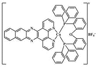
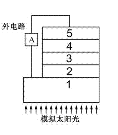
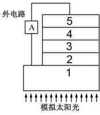
[0023] select figure 2 The battery structure shown. In this embodiment, firstly, an electron donor layer CuPc with a thickness of 15-20 nm is vacuum-deposited on the ITO conductive glass; then, on the electron donor layer 2, the electron donor CuPc and Cu ( I) The mixed layer 3 of the complex has a thickness of 5 nm, and then an electron acceptor layer 4 is deposited on the mixed layer 3 with a thickness of 40 nm; finally, the cathode is made of metal Al material with a thickness of 120 nm. All the above thin films are deposited by vacuum coating process. The thickness of the film is monitored by a film thickness monitoring instrument, and the external circuit is detected by KEITHLEY2601.
[0024] Effect: with a light intensity of 100 mW / cm 2 Under the irradiation of the solar simulator, the obtained current density is 5.57 mA / cm 2 , the open circuit voltage is 0.385 V, the fill factor is 0.384, and the photoelectric conversion efficiency is 0.833%.
Embodiment 2
[0026] On the basis of Example 1, an electron donor layer CuPc with a thickness of 15 to 20 nm is vacuum deposited on the ITO conductive glass, and then electron donor CuPc and Cu with a weight ratio of 100:3 are deposited on the electron donor layer 2 ( I) The mixed layer 3 of the complex has a thickness of 5 nm, and the other fabrication conditions remain unchanged.
[0027] Effect: with a light intensity of 100 mW / cm 2 Under the irradiation of the solar simulator, the obtained current density is 6.213 mA / cm 2 , the open circuit voltage is 0.390 V, the fill factor is 0.379, and the photoelectric conversion efficiency is 0.920 %
Embodiment 3
[0029] On the basis of Example 1, an electron donor layer CuPc with a thickness of 15 to 20 nm was vacuum deposited on the ITO conductive glass, and then electron donor CuPc and Cu with a weight ratio of 100:5 were deposited on the electron donor layer 2 ( I) The mixed layer 3 of the complex has a thickness of 5 nm, and the other fabrication conditions remain unchanged.
[0030] Effect: with a light intensity of 100 mW / cm 2 Under the irradiation of the solar simulator, the obtained current density is 3.157 mA / cm 2 , the open circuit voltage is 0.457 V, the fill factor is 0.374, and the photoelectric conversion efficiency is 0.538%.
PUM
| Property | Measurement | Unit |
|---|---|---|
| thickness | aaaaa | aaaaa |
| thickness | aaaaa | aaaaa |
| thickness | aaaaa | aaaaa |
Abstract
Description
Claims
Application Information


