Double-surface polishing method for gallium antimonide wafer

A double-sided polishing, gallium antimonide technology, applied in surface polishing machine tools, grinding/polishing equipment, electrical components, etc., can solve the problems of reducing MESFET structure, reducing material resistivity uniformity and electron mobility, etc. Strong operability, simple and practical effect

Inactive Publication Date: 2012-07-11
GRINM ELECTRO OPTIC MATERIALS
View PDF10 Cites 15 Cited by
  • Summary
  • Abstract
  • Description
  • Claims
  • Application Information

AI Technical Summary

Problems solved by technology

[0003] The surface damage introduced by wafer surface processing will reduce the uniformity of material resistivity and electron mobility, reduce the uniformity of the source-drain saturation current of the MESFET structure, and the yield and life of the device

Method used


Image

  • Double-surface polishing method for gallium antimonide wafer
  • Double-surface polishing method for gallium antimonide wafer

Examples


Embodiment 1

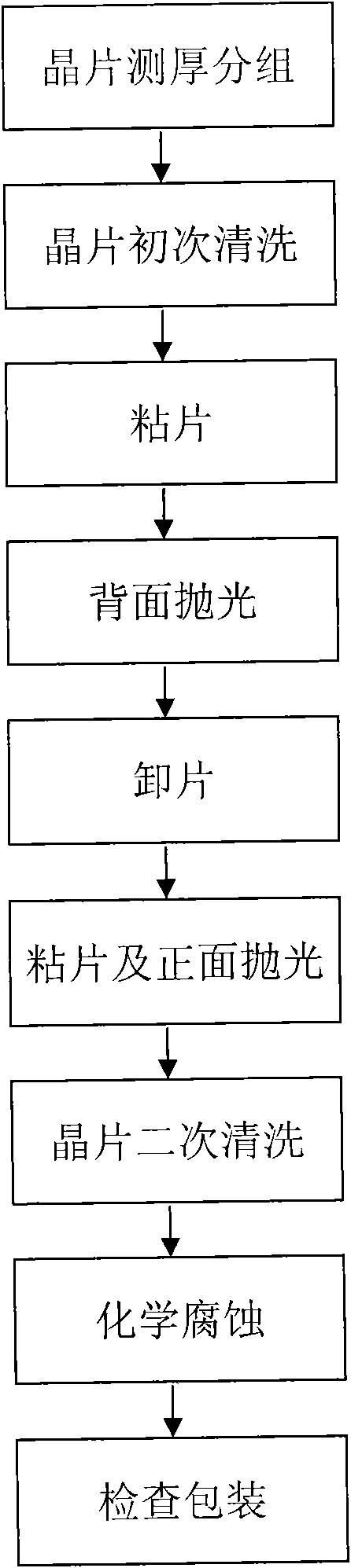
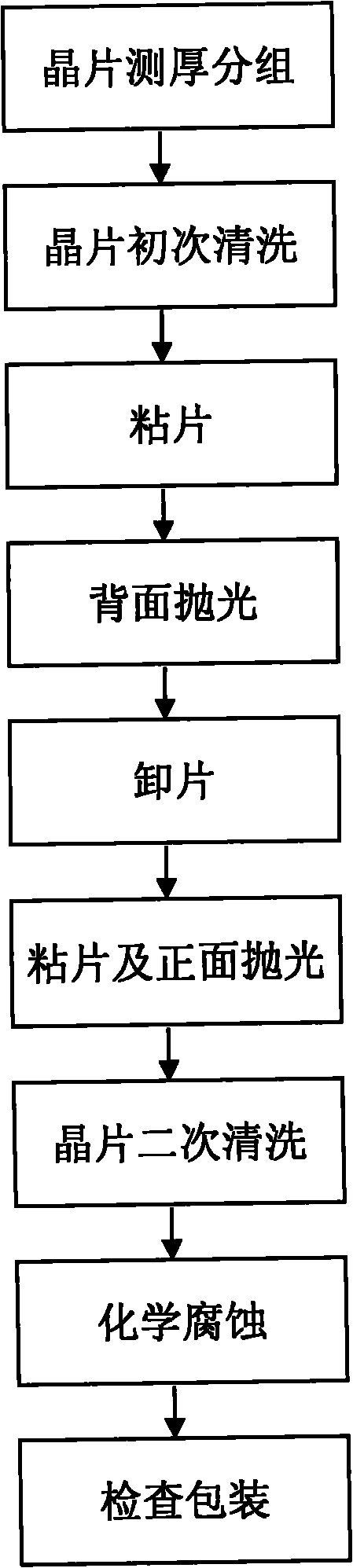
[0028] 1. Wafer thickness measurement grouping: Qualified wafers are divided into grading lines with a thickness difference of 5 μm.

[0029] 2. Initial wafer cleaning: use pure water, H 2 o 2 and NH 4 OH was prepared into an etching solution with a volume ratio of 10:2:1, heated to 30°C, and the wafer was etched in the etching solution for 40 seconds. Rinse with pure water after corrosion, and then dry the water with filter paper.

[0030] 3. Bonding: Carry out front bonding when the surface temperature of the polishing disc is 30°C.

[0031] 4. Backside polishing: use pure water, polishing agent and sodium hypochlorite to prepare a polishing solution at a volume ratio of 90:4:2, set the temperature of the polishing solution at 20°C, set the polishing pressure at 15psi, and the polishing time for 20 minutes. The liquid flow rate was 70 ml / min for backside polishing.

[0032] 5. Unloading: heat the polishing disc to melt the wax layer around the wafer for unloading.

[0...

Embodiment 2

[0038] 1. Wafer thickness measurement and grouping: the qualified wafers are divided into grading lines with a thickness difference of 5-10 μm.

[0039] 2. Initial wafer cleaning: use pure water, H 2 o 2 and NH 4 OH was prepared into an etching solution with a volume ratio of 20:1:5, heated to 40°C, and the wafer was etched in the etching solution for 30 seconds. Rinse with pure water after corrosion, and then dry the water with filter paper.

[0040] 3. Bonding: Carry out front bonding when the surface temperature of the polishing disc is 40°C.

[0041] 4. Back polishing: use pure water, polishing agent and sodium hypochlorite to prepare a polishing liquid in a volume ratio of 70:5:5, set the temperature of the polishing liquid at 45°C, set the polishing pressure at 5 psi, and the polishing time for 30 minutes. The liquid flow rate was 50 ml / min for backside polishing.

[0042] 5. Unloading: Heat the polishing disc to melt the wax layer at the bottom of the wafer for unl...


PUM


Abstract

The invention relates to a double-surface polishing method for a gallium antimonide wafer. The double-surface polishing method comprises the following steps of: grouping wafer thickness measurement; initially cleaning a wafer; adhering the wafer; polishing a back surface; dismantling the wafer; adhering the wafer and polishing a positive surface; secondly cleaning the wafer; placing the wafer with polished double surfaces in a solution prepared from cleaning liquid and purified water in volume ratio of 1:(3-10) for ultrasonic cleaning at 50-100 DEG for 10-30min, washing by using the purified water; corroding chemically: preparing corrosion liquid according to a proportion of CH3COOH, H2O and HF in volume ratio of (10-30):(5-15):1; and checking and packing. According to the double-surface polishing method for the gallium antimonide wafer, disclosed by the invention, the gallium antimonide (100) wafer with polished double surfaces can be machined in batch, the method is simple and practical, the maneuverability is strong, and the polished yield is up to 90%; simultaneously, a problem of oxidation of the polished gallium antimonide wafer is released. The gallium antimonide wafer polished by the double-surface polishing method disclosed by the invention is not larger than 20 microns in warping degree, not larger than 4 microns in wafer surface flatness, 0.1-0.2 micron in surface roughness and not larger than 5 microns in total thickness of the wafer, and the defects of the polished wafer, such as dirt, fog, scratch, particles, cracking, orange peel and crow claw, are not detected.

Description

technical field [0001] The invention relates to a compound semiconductor wafer polishing process, in particular to a gallium antimonide (100) wafer double-sided polishing method. Background technique [0002] Gallium antimonide is an important III-V compound semiconductor material, a good substrate material for electronic and optoelectronic devices, and an excellent material for manufacturing solar cells. Gallium antimonide material has a narrow band gap and a large lattice constant, which is easy to match with semiconductor materials with a band gap, and grows high-quality superlattice and double heterojunction epitaxial layers. It is ideal for manufacturing infrared monitoring devices and Excellent substrate material for quantum well devices. Gallium antimonide material has long been the material of choice for mid-infrared band lasers and detectors, and the wavelength of lasers made of it can be changed within the range of 2-5 μm. In addition to the huge potential applic...

Claims


Application Information

Patent Timeline
Patent Type & Authority Applications(China)
IPC IPC(8): B24B29/02H01L21/304
Inventor 李超林泉郑安生龙彪马锦伟
Owner GRINM ELECTRO OPTIC MATERIALS
Why Eureka
Try Eureka