Thin film solar cell and method for manufacturing the same

The invention relates to a technology of a solar cell and a manufacturing method, which can be applied to circuits, photovoltaic power generation, electrical components, etc., and can solve the problems of insufficient coverage of a buffer layer film, reduced conversion efficiency, and increased carrier recombination probability. The effect of increasing conversion efficiency and reducing leakage current

Inactive Publication Date: 2012-07-11
彭洞清
View PDF1 Cites 13 Cited by
  • Summary
  • Abstract
  • Description
  • Claims
  • Application Information

AI Technical Summary

Problems solved by technology

Although, MoSe 2 The junction can be in ohmic contact, but under the high temperature and high pressure selenization process environment, it often leads to too thick molybdenum layer being converted into MoSe 2 , while too thick MoSe 2 It will lead to an increase in series resistance, and even affect the adhesion of the absorbing layer, causing the absorbing layer to detach or fall off
In addition, if the low-pressure selenization process is used, it can avoid the too thick molybdenum layer from being converted into MoSe 2 , but the formed absorption layer tends to present a granular structure stack, resulting in insufficient flatness and the formation of a rough absorption layer surface, resulting in insufficient coverage of the buffer layer film, resulting in excessive leakage current, resulting in reduced conversion efficiency
In addition, the granular structure stacking of the absorbing layer also increases the probability of carrier recombination and reduces the conversion efficiency.

Method used


Image

  • Thin film solar cell and method for manufacturing the same
  • Thin film solar cell and method for manufacturing the same
  • Thin film solar cell and method for manufacturing the same

Examples


Embodiment 1

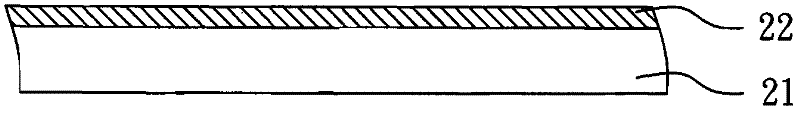
[0024] Such as Figure 2A As shown, a substrate 21 is provided, and a molybdenum layer is deposited on the substrate 21 by sputtering, and the molybdenum layer is used as a first electrode 22 . In this embodiment, the substrate 21 is a glass substrate.

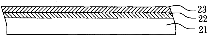
[0025] Then, if Figure 2B As shown, a barrier layer 23 that is conductive and does not easily react with selenium or sulfur is deposited on the first electrode 22 by sputtering or evaporation. In this embodiment, the barrier layer 23 is made of Al. Here, the barrier layer 23 can not only prevent the first electrode 22 from forming selenium or sulfur compounds in the subsequent selenization or sulfurization process, but also can be used as an electrode material because the barrier layer 23 has conductivity.

[0026] Such as Figure 2C As shown, a molybdenum-containing metal layer 24 is deposited on the barrier layer 23 by sputtering. In this embodiment, the molybdenum-containing metal layer 24 is a molybdenum layer, and t...

Embodiment 2

[0032] The thin film solar cell and its manufacturing method in this embodiment are the same as in Embodiment 1, except that the material of the barrier layer 23 in this embodiment is La metal doped with Al. Since the material of the barrier layer 23 in this embodiment is La metal doped with Al, in the subsequent selenization process, the aluminum element in the barrier layer 23 will diffuse to the absorber layer 25a, and then the absorber layer 25a is doped with Al in a gradient. , to achieve a gradient energy gap of the absorbing layer.

Embodiment 3

[0034] The thin-film solar cell and its manufacturing method in this embodiment are the same as in Embodiment 1, except that the material of the molybdenum-containing metal layer 24 in this embodiment is molybdenum metal doped with Al. Since the material of the molybdenum-containing metal layer 24 in this embodiment is molybdenum metal doped with Al, in the subsequent selenization process, the aluminum element in the molybdenum-containing metal layer 24 will diffuse into the absorbing layer 25a, thereby making the absorbing layer 25a have a gradient Al doping, and to achieve a gradient absorption layer energy gap.


PUM


Abstract

The present invention provides a thin film solar cell, which comprises: a substrate; a first electrode disposed on the substrate; a barrier layer disposed on the first electrode, wherein the material of the barrier layer is a conductive material; an ohmic contacting layer disposed on the barrier layer; an absorption layer disposed on the ohmic contacting layer; a buffer layer disposed on the absorption layer; a transparent conductive layer disposed on the buffer layer; and a second electrode disposed on the transparent conductive layer. In addition, the present invention also provides a method for manufacturing the aforementioned thin film solar cell.

Description

technical field [0001] The invention relates to a thin-film solar cell and a manufacturing method thereof, in particular to a copper-indium-selenium-based thin-film solar cell and a manufacturing method thereof. Background technique [0002] With the development of human civilization, the world is facing serious problems such as energy crisis and environmental pollution. Among them, the solar cell, which can directly convert solar energy into electrical energy, is a renewable and environmentally friendly power generation method because it does not generate greenhouse gases such as carbon dioxide and does not pollute the environment during the power generation process. At present, solar cells made of various materials have been developed, such as silicon-based solar cells, dye-sensitized solar cells, and organic material cells. [0003] Among them, the copper indium selenium (CuInSe) solar cell with copper indium gallium selenide (CIGS) or copper indium aluminum selenium (CI...

Claims


Application Information

Patent Timeline
Patent Type & Authority Applications(China)
IPC IPC(8): H01L31/032H01L31/0352H01L31/18
CPCH01L31/0749Y02E10/542H01L31/03923H01L31/0326H01L31/0392H01L31/022408Y02E10/541H01L31/03925H01L31/03928Y02P70/50
Inventor 彭洞清方嘉锋
Owner 彭洞清
Why Eureka
Try Eureka