Waveguide photodetector and forming method thereof

A technology of optical detectors and detectors, applied in semiconductor devices, instruments, optics, etc., can solve the problems of energy coupling, etc., and achieve the effects of reducing defects, solving optical coupling, and no leakage current

Active Publication Date: 2012-07-11
李冰
View PDF1 Cites 8 Cited by
  • Summary
  • Abstract
  • Description
  • Claims
  • Application Information

AI Technical Summary

Problems solved by technology

Due to the difference in refractive index, most of the photons are refracte

Method used


Image

  • Waveguide photodetector and forming method thereof
  • Waveguide photodetector and forming method thereof
  • Waveguide photodetector and forming method thereof

Examples


Embodiment Construction

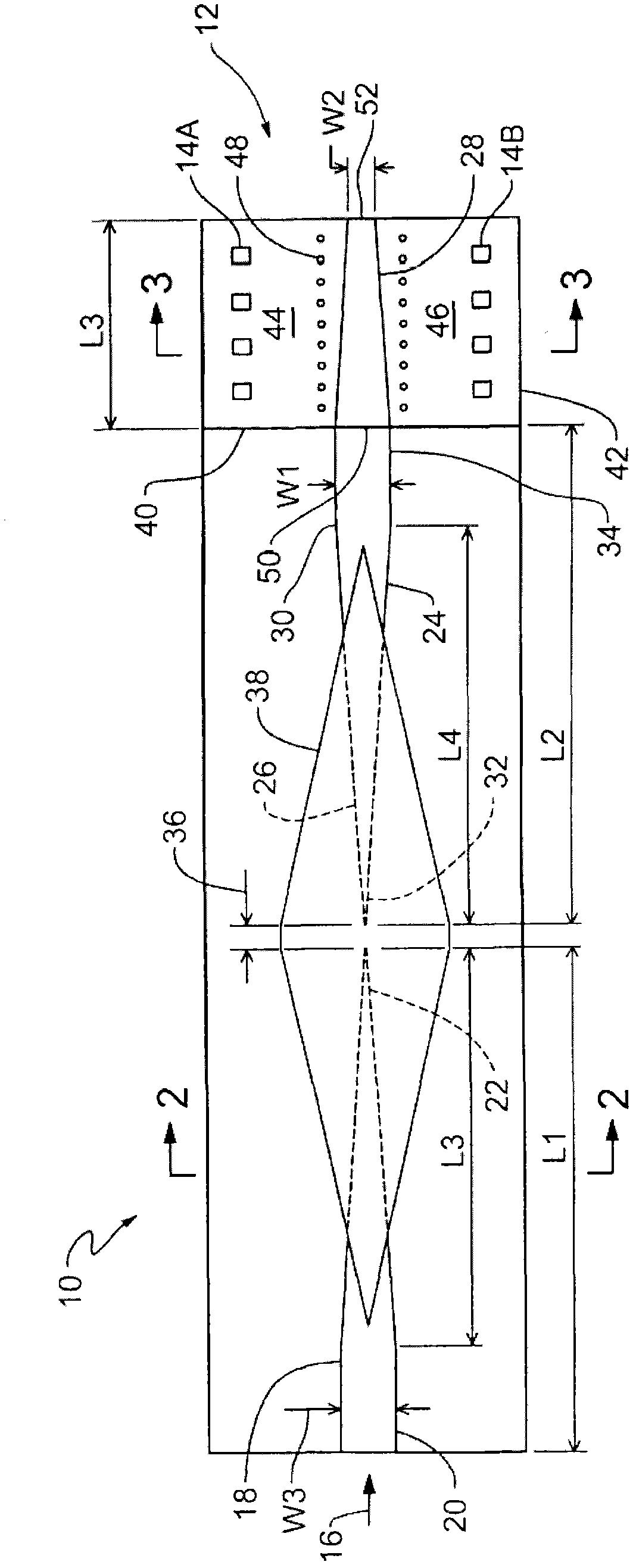
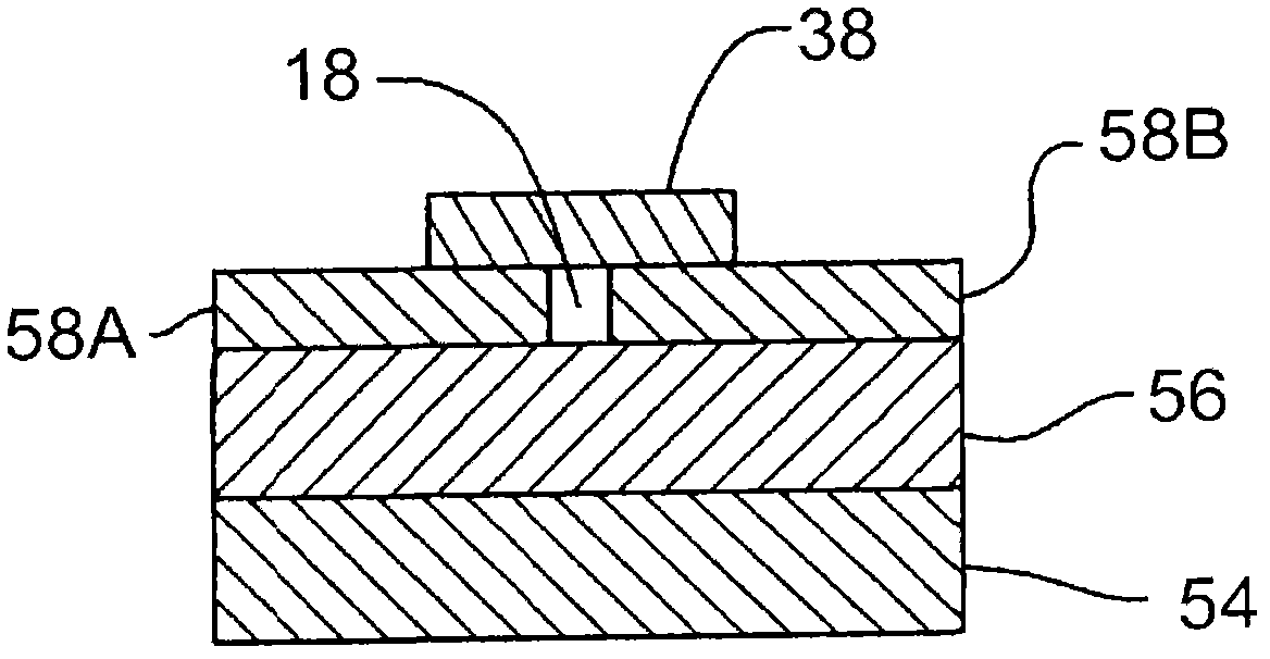
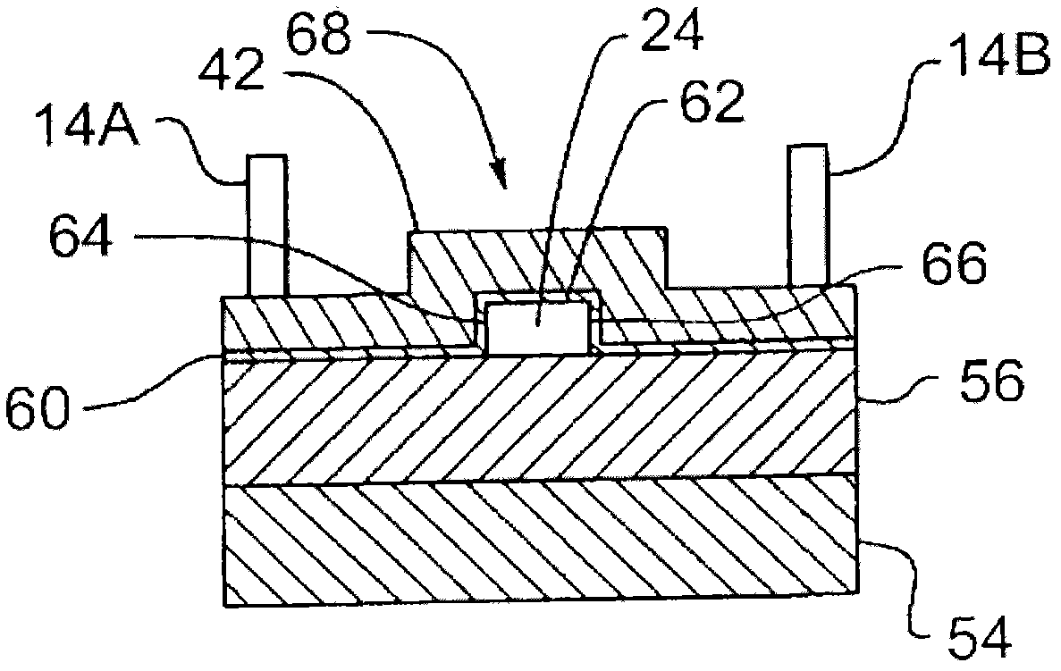
[0057] The invention discloses an improved rapid melting growth technique (RMG) for preparing a waveguide photodetector, and discloses a new RMG-based waveguide photodetector structure. The improved RMG technology deposits the detector material that needs to be crystallized on the silicon waveguide isolated by silicon dioxide, and has only a small germanium seed crystal contact with the bulk silicon layer of the SOI wafer, so that the germanium seed crystal obtained after crystallization The layer has few defects, thereby reducing the leakage current of the waveguide detector.

[0058] figure 1 A top view of one embodiment of the waveguide photodetector disclosed in the present invention is given. As shown in the figure, the waveguide photodetector 10 is a propagation channel of an optical signal, and the optical signal comes from an optical communication system ( figure 1 Not described in ) the light source end is directed by the system to the detection end of the system. ...


PUM


Abstract

A waveguide photodetector and forming method thereof are provided. The method of forming a waveguide photodetector includes: forming a waveguide on a silicon-on-insulator(SOI) substrate(100), depositing a first oxide coating over the waveguide and on the SOI substrate(102), creating a seed window through the first oxide coating to a bulk silicon layer of the SOI substrate(104), depositing a photodetector material into the seed window and on top of the first oxide coating over the waveguide(106), depositing a second oxide coating over the photodetector material and over the first oxide coating deposited over the waveguide and on the SOI substrate(108), and applying thermal energy to liquefy the photodetector material(110). Thereby, the leakage current characteristics of the waveguide photodetector are improved.

Description

technical field [0001] The invention relates to a photoelectric device and a preparation method thereof, in particular to a waveguide photodetector for converting optical signals into electrical signals and a preparation method thereof. Background technique [0002] In an optical communication system, as a propagation channel, an optical waveguide directs and propagates an optical signal generated by a light source (such as a laser) at one end of the optical communication system to a detector (such as a photodetector) at the other end of the system. When light hits the photodetector, the photodetector material as the active region absorbs the energy of photons in the light signal and excites carriers, such as electron-hole pairs. When the photodetector is reverse-biased, the excited carriers are attracted to the electrodes of the photodetector. Thus, a photogenerated current is formed under the action of an external electric field. [0003] Many optical communication syste...

Claims


Application Information

Patent Timeline
IPC IPC(8): H01L31/18H01L31/0232
CPCH01L31/18H01L31/1808H01L31/105H01L31/02325Y02E10/50G02B6/1228H01L31/0232
Inventor 李冰
Owner 李冰
Why Eureka
Try Eureka