Preparation method for high-K medium film

A dielectric thin film and thin film technology, which is applied in the field of high-k dielectric thin film preparation, can solve the problems of difficulty in meeting the high-k dielectric thin film thickness, decreased electrical properties, excessive oxygen vacancies, etc., so as to reduce the equivalent gate oxide thickness and improve the Purity, the effect of suppressing the diffusion of elements

Inactive Publication Date: 2012-07-18
SHANGHAI INST OF MICROSYSTEM & INFORMATION TECH CHINESE ACAD OF SCI
View PDF9 Cites 13 Cited by
  • Summary
  • Abstract
  • Description
  • Claims
  • Application Information

AI Technical Summary

Problems solved by technology

[0006] In view of the shortcomings of the prior art described above, the purpose of the present invention is to provide a method for preparing a high-k dielectric film, which is used to solve the problems of excessively thick interface layers and high-k dielectric films produced in ...

Method used


Image

  • Preparation method for high-K medium film
  • Preparation method for high-K medium film

Examples


Embodiment Construction

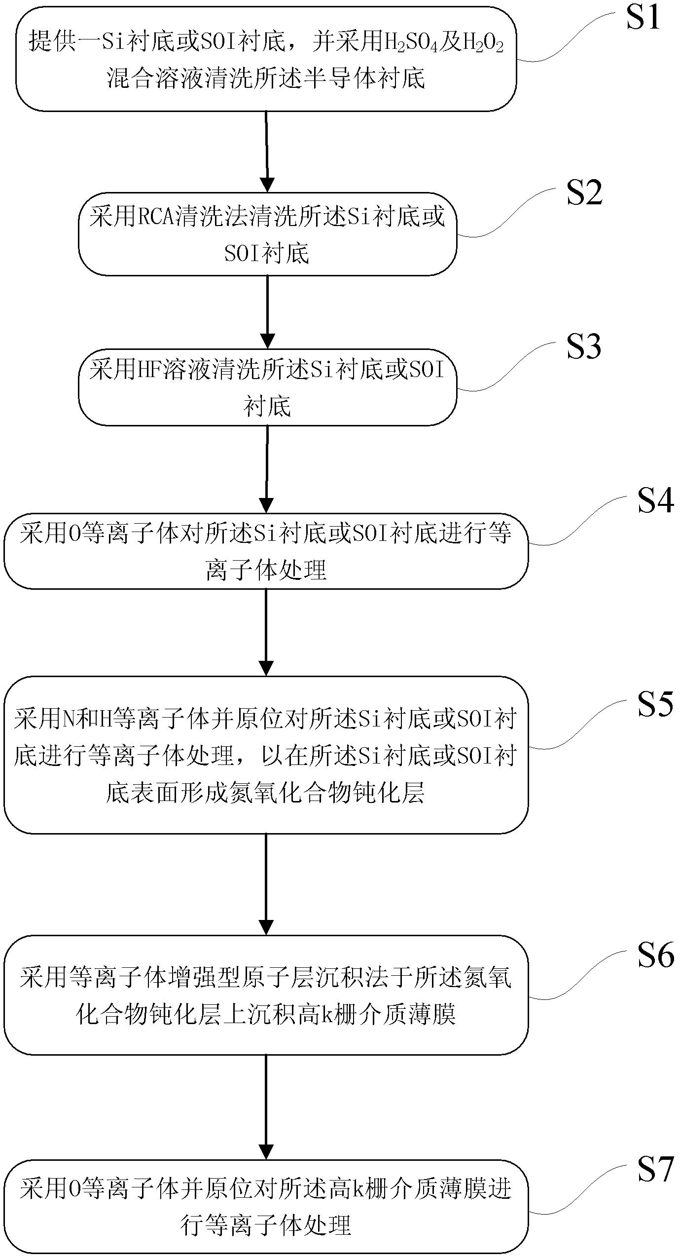
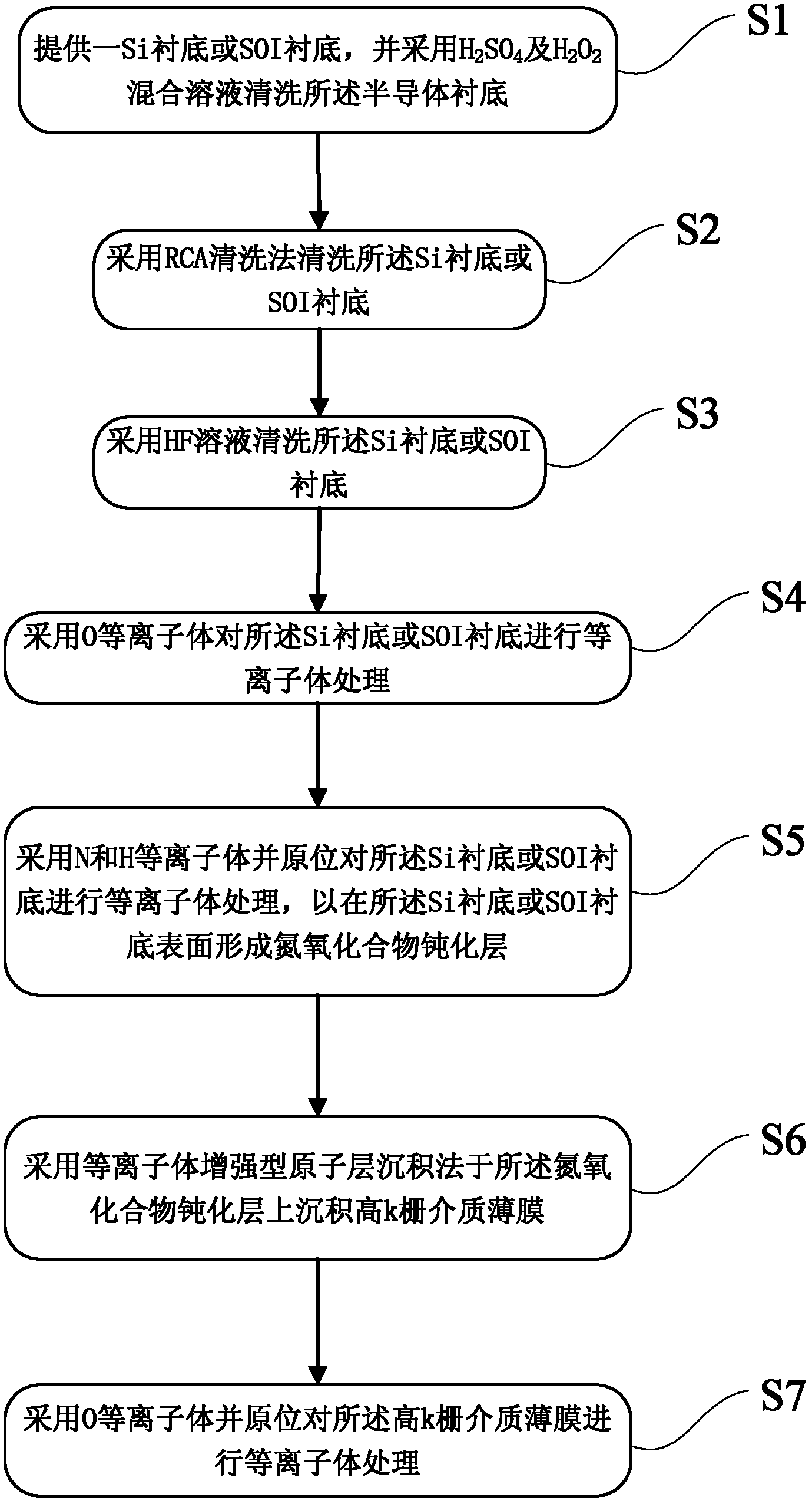
[0027] Embodiments of the present invention are described below through specific examples, and those skilled in the art can easily understand other advantages and effects of the present invention from the content disclosed in this specification. The present invention can also be implemented or applied through other different specific embodiments, and various modifications or changes can be made to the details in this specification based on different viewpoints and applications without departing from the spirit of the present invention.

[0028] see figure 1 . It should be noted that the diagrams provided in this embodiment are only schematically illustrating the basic idea of ​​the present invention, and only the components related to the present invention are shown in the diagrams rather than the number, shape and shape of the components in actual implementation. Dimensional drawing, the type, quantity and proportion of each component can be changed arbitrarily during actual...


PUM


Abstract

The invention provides a preparation method for a high-K medium film. Organics on the surface of a sample can be removed and the purity of the surface of a substrate can be improved by adding the step of washing with H2SO4 and H2O2 before adopting a standard RCA washing method. The thickness of an interface layer of the film can be effectively reduced by removing a surface oxide layer by using hydrogen fluoride (HF) again after adopting the standard RCA washing method. A layer of very thin oxynitride passivation layer grows between the high-K medium film and Si by a plasma atomic layer deposition method and the technology of treating the surface of the Si through in-situ O2 and NH3 plasmas. The high-K medium film passivation layer can inhibit the growth of the interface layer. The high-K medium film is grown in a plasma growing way and oxygen plasma post treatment is performed on the high-K medium film in situ so as to reduce oxygen vacancy in the film. The thickness of an interface buffering layer and the roughness of the interface are reduced by the method, element diffusion between the substrate and the film is inhibited, and equivalent grid oxygen thickness is reduced.

Description

technical field [0001] The invention belongs to the technical field of microelectronics and solid electronics, and in particular relates to a preparation method of a high-k dielectric thin film. Background technique [0002] With the continuous development of large-scale integrated circuit technology, the feature size of metal oxide semiconductor field effect transistor (MOSFET), which is the core device of silicon-based integrated circuits, has been continuously shrinking in accordance with Moore's law. However, the thickness of the MOS tube gate dielectric is getting smaller and smaller, and it is close to its limit. When the thickness of the silicon dioxide gate dielectric is below 10nm (the processing limit of silicon material is generally considered to be 10nm line width), there will be problems such as increased tunneling current, pinhole defects, and poor reliability of performance failure. In order to solve these problems, some integrated circuit research and manufa...

Claims


Application Information

Patent Timeline
IPC IPC(8): H01L21/02H01L21/285
Inventor 程新红曹铎贾婷婷王中健徐大伟夏超宋朝瑞俞跃辉
Owner SHANGHAI INST OF MICROSYSTEM & INFORMATION TECH CHINESE ACAD OF SCI
Why Eureka
Try Eureka