

Transparent resistance random access memory
A resistive memory, resistive memory technology, applied in the direction of electric solid devices, semiconductor devices, electrical components, etc., can solve the problem of not being able to manufacture or apply transparent electronic devices, and achieve low processing costs, stable performance, and good light transmittance. Effect
- Summary
- Abstract
- Description
- Claims
- Application Information
AI Technical Summary
Problems solved by technology
Method used
Image

Examples
Embodiment 1
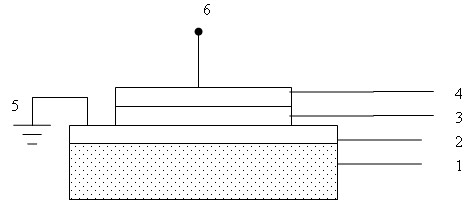
[0023] (1) Deposit aluminum-doped zinc oxide lower electrode 2 on a colorless and transparent glass substrate 1 by radio frequency magnetron sputtering:
[0024] The back vacuum of the sputtering chamber is 10 -5 Pa, with aluminum-doped zinc oxide as the target material, the sputtering gas is argon, the sputtering pressure is 1Pa, the sputtering power is 300W, and the sputtering time is 10 minutes, so that the thickness of the lower electrode 2 is 50nm. The atomic percent content of aluminum is 1%.
[0025] (2) Depositing a magnesium-doped zinc oxide resistive storage layer 3 on the lower electrode 2 by radio frequency magnetron sputtering:
[0026] The back vacuum of the sputtering chamber is 10 -5 Pa, with magnesium-doped zinc oxide as the target material, the sputtering gas is argon and oxygen gas mixture (flow ratio 98:2), the sputtering pressure is 1Pa, the sputtering power is 300W, and the sputtering time is 30 minutes. The thickness of the variable storage layer 3 is...
Embodiment 2
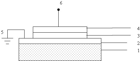
[0032] (1) Deposit aluminum-doped zinc oxide lower electrode 2 on polycarbonate substrate 1 by radio frequency magnetron sputtering method:
[0033] The back vacuum of the sputtering chamber is 10 -5 Pa, with aluminum-doped zinc oxide as the target material, the sputtering gas is argon, the sputtering pressure is 1Pa, the sputtering power is 300W, and the sputtering time is 20 minutes, so that the thickness of the lower electrode 2 is 80nm. The atomic percent content of aluminum is 3%.
[0034] (2) Depositing a magnesium-doped zinc oxide resistive storage layer 3 on the lower electrode 2 by radio frequency magnetron sputtering:
[0035] The back vacuum of the sputtering chamber is 10 -5 Pa, with magnesium-doped zinc oxide as the target material, the sputtering gas is argon and oxygen gas mixture (flow ratio 98:2), the sputtering pressure is 1Pa, the sputtering power is 300W, and the sputtering time is 40 minutes. The thickness of the variable storage layer 3 is 120nm, and t...
Embodiment 3
[0041] (1) Using the radio frequency magnetron sputtering method, deposit gallium-doped zinc oxide lower electrode 2 on a colorless and transparent polymethyl methacrylate substrate 1:
[0042] The back vacuum of the sputtering chamber is 10 -5 Pa, with gallium-doped zinc oxide as the target material, the sputtering gas is argon, the sputtering pressure is 1Pa, the sputtering power is 300W, and the sputtering time is 10 minutes, so that the thickness of the lower electrode 2 is 50nm. The atomic percent content of gallium is 4%.
[0043] (2) Deposit a beryllium-doped zinc oxide resistive storage layer 3 on the bottom electrode 2 by radio frequency magnetron sputtering:
[0044] The back vacuum of the sputtering chamber is 10 -5 Pa, with beryllium-doped zinc oxide as the target material, the sputtering gas is argon and oxygen gas mixture (flow ratio 98:2), the sputtering pressure is 1Pa, the sputtering power is 300W, and the sputtering time is 50 minutes. The variable storag...
PUM
| Property | Measurement | Unit |
|---|---|---|
| Thickness | aaaaa | aaaaa |
| Thickness | aaaaa | aaaaa |
| Thickness | aaaaa | aaaaa |
Abstract
Description
Claims
Application Information