

Ultraviolet-light gallium nitride semiconductor light emitting diode with gradient electron barrier layers
A technology of light-emitting diodes and electron blocking layers, which is applied in semiconductor devices, circuits, electrical components, etc., can solve the problems that the quantum efficiency of ultraviolet semiconductor light-emitting diodes is difficult to improve, and achieve the improvement of quantum efficiency and luminous efficiency, optimize the energy band structure, and improve Effect of Injection Efficiency
- Summary
- Abstract
- Description
- Claims
- Application Information
AI Technical Summary
Problems solved by technology
Method used
Image

Examples
Embodiment approach 1
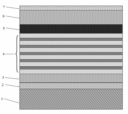
[0017] 1) Grow a gallium nitride layer (9) on the sapphire substrate (8), the growth temperature is between 500-600 degrees Celsius, the optimum temperature is around 540 degrees Celsius, the growth pressure is between 300Torr-700Torr, the optimum Good for 500Torr. The thickness of the gallium nitride layer (9) is between 15nm and 100nm, preferably controlled at 25nm. See attached Figure 8 .
[0018] 2) A non-doped gallium nitride layer (10) is grown on the gallium nitride layer (9). Good for 300Torr. The thickness of the gallium nitride layer (10) is 500-5000nm, and 2500nm is the optimal thickness. See attached Figure 8 .
[0019] 3) An N-type gallium nitride layer (11) is grown on the gallium nitride layer (10), and the doping impurity is simple silicon, and the doping concentration is between 1E18-1E19 per cubic centimeter. The growth temperature range of the gallium nitride layer (11) is 1000-1100 degrees Celsius, the optimal temperature is 1050 degrees Celsius, t...
Embodiment approach 2
[0027] 1)-4) and 6)-7) are the same as one of the embodiment modes, only the embodiment mode 5), that is, the graded aluminum composition AlGaN electron blocking layer is different.
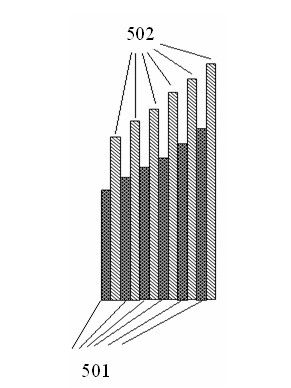
[0028] 5) A P-type aluminum gallium nitrogen AlyGa1-yN electron blocking layer (13) is grown on the active layer (12), doped with metal magnesium as an impurity, and the doping concentration is on the order of 1E19-5E20 per cubic centimeter. The growth temperature is between 850-1000 degrees Celsius, 960 degrees Celsius is the optimal growth temperature, and the growth pressure is between 50-500 Torr, preferably controlled at 100 Torr. The second design of the AlGaN electron blocking layer (5) described in the content of the invention 8) is realized through the control of the aluminum source. The specific changes are as follows (see attached image 3 shown): the thin AlGaN layer (501) is an AlGaN layer with a thickness of 1 nm and an Al composition of 0.6-0.02*x, and the thin AlGaN layer (502) is ...
Embodiment approach 3
[0030] 1)-4) and 6)-7) are the same as one of the embodiment modes, only the embodiment mode 5), that is, the graded aluminum composition AlGaN electron blocking layer is different.
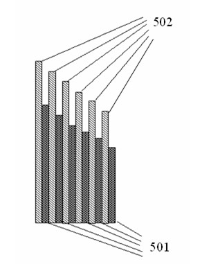
[0031] 5) A P-type aluminum gallium nitrogen AlyGa1-yN electron blocking layer (13) is grown on the active layer (12), doped with metal magnesium as an impurity, and the doping concentration is on the order of 1E19-5E20 per cubic centimeter. The growth temperature is between 850-1000 degrees Celsius, 960 degrees Celsius is the optimal growth temperature, and the growth pressure is between 50-500 Torr, preferably controlled at 100 Torr. The third design of the AlGaN electron blocking layer (5) described in the content of the invention 8) is realized through the control of the aluminum source. The specific changes are as follows (see attached Figure 4 shown): the thin AlGaN layer (501) is 1 nanometer thick and the aluminum composition is 0.6-0.02*x (xx_mid) ), the thin AlGaN layer (502) is 1 nan...
PUM
| Property | Measurement | Unit |
|---|---|---|
| Thickness | aaaaa | aaaaa |
| Thickness | aaaaa | aaaaa |
Abstract
Description
Claims
Application Information