Microelectrode array sensor as well as preparation method and stripping voltmeter detection method thereof
A technology of microelectrode array and stripping voltammetry, which is applied in the field of sensors, can solve the problems of poor consistency of test results and achieve good consistency, good signal-to-noise ratio, and simple and portable instruments
- Summary
- Abstract
- Description
- Claims
- Application Information
AI Technical Summary
Problems solved by technology
Method used
Image
Examples
Embodiment 1
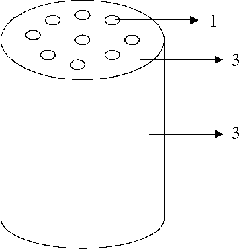
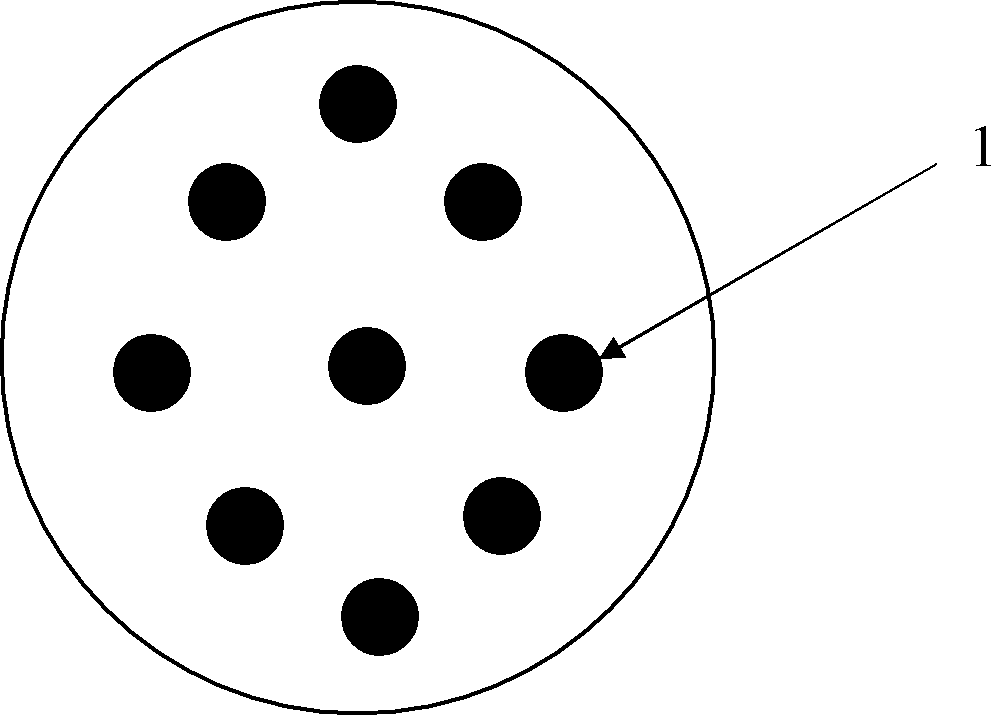
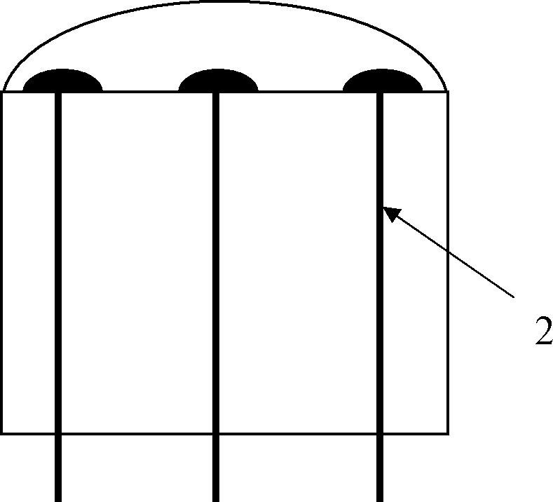
[0055] Such as figure 1 , the microelectrode array sensor shown in Fig. 2 (a), Fig. 2 (b), comprise active point 1, conductive fiber 2 and insulator 3, active point is positioned at insulator top surface, conductive fiber passes through insulator and connects active point; Active point The diameter is 10 microns, and the conductive fiber includes a metal wire and an insulating material wrapped around the metal wire.
[0056] The insulator is cylindrical. There are 9 active points, one is located at the center of the top surface, and the rest are arranged around the center of the circle.
[0057] The material of the active point is: one or any combination of carbon fiber, glassy carbon, carbon nanotube, graphene, fullerene, diamond, gold, platinum, bismuth, boron.
[0058] The preparation method of the microelectrode array sensor is a photolithography method, and the photolithography method includes the following steps:
[0059] Such as image 3 As shown, the lithography st...
Embodiment 2
[0086] Such as Figure 5 as shown, Figure 5 It is the cyclic voltammogram of the microelectrode array sensor of the present invention in 0.01mol / L K3[Fe(CN)6]0.1mol / L KCl solution. The results of this implementation show that the microelectrode array has a spherical diffusion model response. It is very small, and the edge part is relatively close to the solution, and the replenishment of electroactive substances is relatively fast.
[0087] Figure 5 It reflects the basic electrochemical characteristics of the array microelectrode, and the current is very small in the cyclic voltammetry scan in the solution.
Embodiment 3
[0089] Image 6 is the microelectrode array of the present invention at 50ppb Pb 2+ Responses on different electrodes under different conditions, where:
[0090] a curve is the response of glassy carbon electrode (existing electrode) without stirring condition;
[0091] The b curve is the response of the glassy carbon electrode (existing electrode) under stirring conditions;
[0092] Curve c is the response of the carbon fiber array microelectrode (electrode of the present invention) without stirring.
[0093] The result of this implementation shows that the microelectrode array of the present invention does not need to be stirred, and has relatively high sensitivity.
PUM
| Property | Measurement | Unit |
|---|---|---|
| Diameter | aaaaa | aaaaa |
Abstract
Description
Claims
Application Information
 - R&D Engineer
- R&D Manager
- IP Professional
- Industry Leading Data Capabilities
- Powerful AI technology
- Patent DNA Extraction
Browse by: Latest US Patents, China's latest patents, Technical Efficacy Thesaurus, Application Domain, Technology Topic, Popular Technical Reports.
© 2024 PatSnap. All rights reserved.Legal|Privacy policy|Modern Slavery Act Transparency Statement|Sitemap|About US| Contact US: help@patsnap.com


